
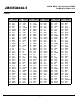
Datasheet


J
J
J
M
M
M
3
3
3
3
3
3
5
5
5
Q
Q
Q
6
6
6
4
4
4
4
4
4
A
A
A
-
-
-
5
5
5
240PIN DDR2 533 Unbuffered DIMM
256MB With 32Mx16 CL4
Transcend Information Inc.
7
Input AC Logic Level
Parameter Symbol Min Max Unit Note
Input High (Logic 1) Voltage, DQ, DQS and DM signals VIH(AC) VREF + 0.250 V
Input Low (Logic 0) Voltage, DQ, DQS and DM signals VIL(AC) VREF - 0.250 V
AC Input Test Condition
Condition Symbol Value Unit Note
Input reference voltage VREF 0.5*VDDQ V 1
Input signal maximum peak to peak swing VSWING(MAX) 1.0 V 1
Input signal minimum slew rate SLEW
1.0 V/ns 2,3
1. Input waveform timing is referenced to the input signal crossing through the VIH/IL(AC) level applied to the
device under test.
2. The input signal minimum slew rate is to be maintained over the range from VREF to VIH(AC) min for rising
edges and the range from VREF to VIL(AC) max for falling edges as shown in the below figure.
Note:
3. AC timings are referenced with input waveforms switching from VIL(AC) to VIH(AC) on the positive transitions
and VIH(AC) to VIL(AC) on the negative transitions.
V
SWING(MAX)
delta TF
delta TR
VDD
V
IH
(AC)
min
V
IH
(DC)
min
VREF
V
IL
(DC)
max
V
IL
(AC)
max
VSS
Falling Slew=
V
REF
-V
IL
(AC)
max
delta TF
Rising Slew=
V
IH
(AC)
min-
V
REF
delta TR
AC Input Test Signal Waveform
Input/Output Capacitance
(VDD = 1.8V, VDDQ = 1.8V, TA = 25°C)
Parameter Symbol Min Max Unit
Input capacitance (CK0 and /CK0)
Input capacitance (CKEx , /CSx and ODTx)
Input capacitance (A0~A12, BA0~BA2, /RAS, /CAS, /WE)
Input capacitance (DQ, DM, DQS, /DQS)
C
CK
CI1
CI2
CIO
-
--
-
-
38
17
37
8
pF
pF
pF
pF
Note:
DM is internally loaded to match DQ and DQS identically.