TS2G~16GMSA500 TS16G~64GMSA300 mSATA SSD Features Description The Transcend TSxGMSA500/TSxGMSA300 is a • RoHS compliant series of mSATA SSD device with high performance and • Power Supply: 3.3V±5% quality Flash Memory assembled on a printed circuit • Operating Temperature: 0oC to 70oC board. These devices feature cutting-edge technique to • Storage Temperature: -40oC to 85oC enhance product life and data retention.
TS2G~16GMSA500 TS16G~64GMSA300 mSATA SSD Specifications Physical Specification Form Factor MO-300 Storage Capacities 2GB~64GB Dimensions (mm) Length 50.8 ± 0.15 Width 29.85 ± 0.15 Height 3.5 ± 0.1 Input Voltage 3.
TS2G~16GMSA500 TS16G~64GMSA300 mSATA SSD ® Note:25 ℃, Typical value, test on ASUS P4S800-MX, 1GB RAM, Windows XP Version 2002 SP2, benchmark utility HDBENCH (version 3.4006), copied file 1GB Actual Capacity Model P/N User Max. LBA Cylinder Head Sector TS2GMSA500 3,865,680 3,835 16 63 TS4GMSA500 7,732,368 7,671 16 63 TS8GMSA500 15,465,344 15,343 16 63 TS16GMSA500 30,932,992 16,383 15 63 TS16GMSA300 30,932,992 16,383 15 63 TS32GMSA300 61,865,984 16.
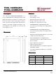
TS2G~16GMSA500 TS16G~64GMSA300 mSATA SSD Package Dimensions Below figure illustrates the Transcend mSATA Solid State Disk product. All dimensions are in mm. Transcend Information Inc. 4 V1.
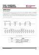
TS2G~16GMSA500 TS16G~64GMSA300 mSATA SSD Pin Assignments Pin No. Pin Name Pin No. Pin Name 01 NC 02 3.3V 03 NC 04 GND 05 NC 06 NC 07 NC 08 NC 09 GND 10 NC 11 NC 12 NC 13 NC 14 NC 15 GND 16 NC 17 NC 18 GND 19 NC 20 NC 21 GND 22 NC 23 TX+ 24 3.3V 25 TX- 26 GND 27 GND 28 NC 29 GND 30 NC 31 RX- 32 NC 33 RX+ 34 GND 35 GND 36 NC 37 GND 38 NC 39 3.3V 40 GND 41 3.
TS2G~16GMSA500 TS16G~64GMSA300 mSATA SSD Block Diagram mSATA Interface SATA Flash CTL Flash Transcend Information Inc. Flash Flash Flash 6 V1.
TS2G~16GMSA500 TS16G~64GMSA300 mSATA SSD Reliability Wear-Leveling algorithm The controller supports static/dynamic wear leveling. When the host writes data, the controller will find and use the block with the lowest erase count among the free blocks. This is known as dynamic wear leveling. When the free blocks' erase count is higher than a threshold value plus data blocks', it will activate the static wear leveling, replacing the not so frequently used user blocks with the high erase count free blocks.
TS2G~16GMSA500 TS16G~64GMSA300 mSATA SSD mSATA Interface Out of bank signaling There shall be three Out Of Band (OOB) signals used/detected by the Phy: COMRESET, COMINIT, and COMWAKE. COMINIT, COMRESET and COMWAKE OOB signaling shall be achieved by transmission of either a burst of four Gen1 ALIGNP primitives or a burst composed of four Gen1 Dwords with each Dword composed of four D24.3 characters, each burst having a duration of 160 UIOOB.
TS2G~16GMSA500 TS16G~64GMSA300 mSATA SSD COMRESET COMRESET always originates from the host controller, and forces a hardware reset in the device. It is indicated that transmitting bursts of data separated by an idle bus condition. The OOB COMRESET signal shall consist of no less than six data bursts, including inter-burst temporal spacing.
TS2G~16GMSA500 TS16G~64GMSA300 mSATA SSD Description: 1. Host/device is powered and operating normally with some form of active communication. 2. Some condition in the host causes the host to issue COMRESET 3. Host releases COMRESET. Once the condition causing the COMRESET is released, the host releases the COMRESET signal and puts the bus in a quiescent condition. 4. Device issues COMINIT – When the device detects the release of COMRESET, it responds with a COMINIT.
TS2G~16GMSA500 TS16G~64GMSA300 mSATA SSD COMINIT COMINIT always originates from the drive and requests a communication initialization. It is electrically identical to the COMRESET signal except that it originates from the device and is sent to the host. The device uses it to request a reset from the host in accordance to the sequence shown in Figure 6, below. Figure 6: cominit sequence Description: 1. Host/device are powered and operating normally with some form of active communication. 2.
TS2G~16GMSA500 TS16G~64GMSA300 mSATA SSD times.) This step is repeated for as many slower speeds as are supported. Once the lowest speed has been reached without response from the host, the device enters an error state. 5. Host locks – after detecting the COMWAKE, the host starts transmitting D10.2 characters at its lowest supported rate. Meanwhile, the host receiver locks to the ALIGN sequence and, when ready, returns the ALIGN sequence to the device at the same speed as received.
TS2G~16GMSA500 TS16G~64GMSA300 mSATA SSD Description: 1. Host/device power-off - Host and device power-off. 2. Power is applied - Host side signal conditioning pulls TX and RX pairs to neutral state (common mode voltage). 3. Host issues COMRESET 4. Host releases COMRESET. Once the power-on reset is released, the host releases the COMRESET signal and puts the bus in a quiescent condition. 5. Device issues COMINIT – When the device detects the release of COMRESET, it responds with a COMINIT.
TS2G~16GMSA500 TS16G~64GMSA300 mSATA SSD ATA command register This table with the following paragraphs summarizes the ATA command set.
TS2G~16GMSA500 TS16G~64GMSA300 mSATA SSD ATA Command Specifications FLUSH CACHE (E7h) The host uses this command to request the device to flush the write cache. If there is data in the write cache, that data shall be written to the media. The BSY bit shall remain set to one until all data has been successfully written or an error occurs. IDENTIFY DEVICE (ECh) This commands read out 512Bytes of drive parameter information.
TS2G~16GMSA500 TS16G~64GMSA300 mSATA SSD Identify Device Information Default Value Word Address Default Value Total Bytes 48 0000h 2 Reserved 49 0F00h 2 Capabilities 50 4000h 2 Capabilities Data Field Type Information 51 0200h 2 PIO data transfer cycle timing mode 52 0000h 2 Obsolete 53 0007h 2 Field Validity 54 XXXXh 2 Current numbers of cylinders 55 00XXh 2 Current numbers of heads 56 XXXXh 2 Current sectors per track 57-58 XXXXh 4 Current capacity in sectors (
TS2G~16GMSA500 TS16G~64GMSA300 mSATA SSD Identify Device Information Default Value Word Address Default Value Total Bytes 93-127 0000h 70 Reserved 128 0001h 2 Security status 129-159 0000h 64 Vendor unique bytes 160 81F4h 2 Power requirement description 161 0000h 2 Reserved 162 0000h 2 Key management schemes supported 163 0000h 2 CF Advanced True IDE Timing Mode Capability and Setting 164 0000h 2 Reserved 165-175 0000h 22 Reserved 176-255 0000h 140 Reserved Data
TS2G~16GMSA500 TS16G~64GMSA300 mSATA SSD transfer of a block, which contains the number of sectors defined by Set Multiple command. WRITE SECTOR(S) (30h) Write data to a specified number of sectors (1 to 256, as specified with the Sector Count register) from the specified address. Specify “00h” to write 256 sectors. NOP (00h) The device shall respond with command aborted. For devices implementing the Overlapped feature set, subcommand code 00h in the Features register shall abort any outstanding queue.
TS2G~16GMSA500 TS16G~64GMSA300 mSATA SSD Security Mode Feature Set SECURITY SET PASSWORD (F1h) This command set user password or master password. The host outputs sector data with PIO data-out protocol to indicate the information defined in the following table.
TS2G~16GMSA500 TS16G~64GMSA300 mSATA SSD This command shall be issued immediately before the Security Erase Unit command to enable erasing and unlocking. This command prevents accidental loss of data on the drive. SECURITY ERASE UNIT (F4h) The host uses this command to transfer 512 bytes of data, as shown in the following table, to the drive. The transferred data contains a user or master password, which the drive compares with the saved password.
TS2G~16GMSA500 TS16G~64GMSA300 mSATA SSD This command disables all SMART capabilities including any and all timer and event count functions related exclusively to this feature. After command acceptance, this controller will disable all SMART operations. SMART data in no longer be monitored or saved. The state of SMART is preserved across power cycles. SMART ENABLE/DISABLE ATTRIBUTE AUTOSAVE B0h with a Feature register value of D2h.Enables or disables the attribute value autosave function.
TS2G~16GMSA500 TS16G~64GMSA300 mSATA SSD Byte 0-1 2 - 361 362 363 364 - 365 366 367 368 - 369 F/V X X V X V X F F Description Revision code Vender specific Off-line data collection status Self-test execution status byte Total time in second to complete off-line data collection activity Vendor specific Off-line data collection capability SMART capability 370 F Error logging capability ‧7 - 1 Reserved ‧0 1 = Device error logging supported 371 372 373 374 375 - 385 386 - 395 396 - 397 398 - 399 400 - 4
TS2G~16GMSA500 TS16G~64GMSA300 mSATA SSD The above technical information is based on industry standard data and has been tested to be reliable. However, Transcend makes no warranty, either expressed or implied, as to its accuracy and assumes no liability in connection with the use of this product. Transcend reserves the right to make changes to the specifications at any time without prior notice USA Los Angeles: E-mail: sales@transcendusa.com Maryland: E-mail: sales_md@transcendusa.com www.transcendusa.