
Datasheet


T
T
T
S
S
S
1
1
1
6
6
6
M
M
M
L
L
L
D
D
D
6
6
6
4
4
4
V
V
V
6
6
6
D
D
D
5
5
5
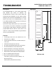
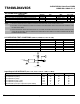
184PIN DDR266 Unbuffered DIMM
128MB With 16Mx8 CL2.5
Dimensions
Side Millimeters Inches
A 133.35±0.20 5.250±0.008
B 72.39 2.850
C 6.35 0.250000
D 2.20 0.0870
E 31.75±0.20 1.250±0.00800
F 19.80 0.779
G 4.00 0.157
H 12.00 0.472
I 1.27±0.10 0.050±0.004
(Refer Placement)
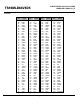
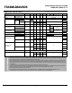
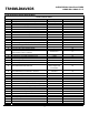
Pin Identification
Symbol Function
A0~A11, BA0, BA1 Address input
DQ0~DQ63 Data Input / Output.
DQS0~DQS7 Data strobe input/output
CK0, /CK0, CK1, /CK1
CK2, /CK2
Clock Input.
CKE0 Clock Enable Input.
/CS0 Chip Select Input.
/RAS Row Address Strobe
/CAS Column Address Strobe
/WE Write Enable
DM0~DM7 Data-in Mask
VDD +2.5 Voltage power supply
VDDQ +2.5 Voltage Power Supply for DQS
VREF Power Supply for Reference
VDDSPD +2.5 Voltage Serial EEPROM
Power Supply
SA0~SA2 Address in EEPROM
SCL Serial PD Clock
SDA Serial PD Add/Data input/output
VSS Ground
NC No Connection
Transcend Information Inc.
2