
Datasheet


T
T
T
S
S
S
1
1
1
6
6
6
M
M
M
L
L
L
D
D
D
6
6
6
4
4
4
V
V
V
6
6
6
D
D
D
5
5
5
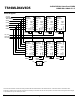
184PIN DDR266 Unbuffered DIMM
128MB With 16Mx8 CL2.5
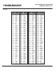
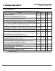
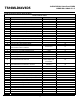
AC Timing Parameters & Specifications
(These AC characteristics were tested on the Component)
Parameter Symbol Min Max Unit Note
Row cycle time tRC 65 ns
Refresh row cycle time tRFC 75 ns
Row active time tRAS 45 120K ns
/RAS to /CAS delay tRCD 20 ns
Row active to Row active delay tRP 20 ns
Row active to Row active delay tRRD 15 ns
Write recovery time tWR 15 ns
Last data in to Read command tWTR 1 tCK
Col. Address to Col. Address delay tCCD 1 tCK
Clock cycle time tCK 7.5 ns
Clock high level width tCH 0.45 0.55 tCK
Clock low level width tCL 0.45 0.55 tCK
DQS-out access time from CK /CK tDQSCK -0.75 0.75 ns
Output data access time from CK /CK tAC -0.75 0.75 ns
Data strobe edge to output data edge tDQSQ 0.5 ns
Read Preamble tRPRE 0.9 1.1 tCK
Read Postamble tRPST 0.4 0.6 tCK
CK to valid DQS-in tDQSS 0.75 1.25 tCK
DQS-in setup time tWPRES 0 ns 2
DQS-in hold time tWPREH 0.25 tCK
DQS falling edge to CK rising-setup time tDSS 0.2 tCK
DQS falling edge from CK rising-hold time tDSH 0.2 tCK
DQS-in high level width tDQSH 0.35 tCK
DQS-in low level width tDQSL 0.35 tCK
DQS-in cycle time tDSC 0.9 1.1 tCK
Address and Control input setup time tIS 0.9 ns
Address and Control input hold time tIH 0.9 ns
Data-out high-impedance time from CK, /CK tHZ tACmin-400ps tACman-400ps ns
Data-out low-impedance time from CK, /CK tLZ tACmin-400ps tACman-400ps ns
Mode register set cycle time tMRD 15 ns
DQ & DM setup time to DQS tDS 0.5 ns
DQ & DM hold time to DQS tDH 0.5 ns
DQ & DM input pulse width tDIPW 1.75 ns
Power down exit time tPDEX 7.5 ns
Exit self refresh to write command tXSW ns
Exit self refresh to bank active command tXSA 75 ns
Exit self refresh to read command tXSR 200 tCK
Refresh interval time tREF 15.6 us 1
Clock half period tHP tCLmin or
tCHmin
ns
Data hold skew factor tQHS 0.75 ns
DQS write postamble time tWPST 0.4 0.6 tCK 3
Note: 1. Maximum burst refresh of 8
2. The specific requirement is that DQS be valid (High or Low) on or before this CK edge. The case shown
(DQS going from High_Z to logic Low) applies when no writes were previously in progress on the bus. If a
previous write was in progress, DQS could be High at this time, depending on tDQSS.
3. The Maximum limit for this parameter is not a device limit. The device will operate with a great value for this
parameter, but system performance (bus turnaround) will degrade accordingly.
Transcend Information Inc.
8