
Datasheet

T
T
T
S
S
S
3
3
3
2
2
2
M
M
M
L
L
L
Q
Q
Q
6
6
6
4
4
4
V
V
V
4
4
4
M
M
M
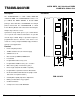
240PIN DDR2 400 Unbuffered DIMM
256MB With 32Mx16 CL3
Transcend Information Inc.
2
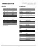
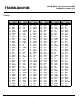
Dimensions
Side Millimeters Inches
A 133.35±0.15 5.250±0.006
B 55 2.165
C 63 2.480000
D 5 0.197
E 2.5 0.0980
F 1.5±0.10 0.059±0.039
G 5.175 0.204
H 2.2 0.867
I 4 0.157
J 10 0.394
K 17.8 0.701
L 30.0±0.15 1.181±0.006
M 1.27±0.10 0.050±0.004
(Refer Placement)
Pin Identification
Symbol Function
A0~A12, BA0, BA1 Address input
DQ0~DQ63 Data Input / Output.
DQS0~DQS7 Data strobe
/DQS0~/DQS7 Differential Data strobe
CK0, /CK0
CK1, /CK1
Clock Input.
CKE0 Clock Enable Input.
ODT0 On-die termination control line
/CS0 Chip Select Input.
/RAS Row Address Strobe
/CAS Column Address Strobe
/WE Write Enable
DM0~DM7 Data-in Mask
VDD +1.8 Voltage power supply
VDDQ
+1.8 Voltage Power Supply for
DQS
VREF Power Supply for Reference
VDDSPD
Serial EEPROM Positive Power
Supply
SA0~SA2 Address select for EEPROM
SCL Serial PD Clock
SDA Serial PD Add/Data input/output
VSS Ground
NC No Connection