
Datasheet

T
T
T
S
S
S
3
3
3
2
2
2
M
M
M
L
L
L
R
R
R
7
7
7
2
2
2
V
V
V
6
6
6
F
F
F
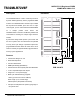
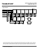
168PIN PC133 Registered DIMM
256MB With 32Mx8 CL3
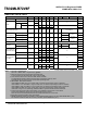
Serial Presence Detect Specification
Serial Presence Detect
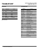
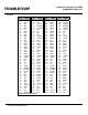
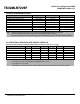
Byte No. Function Described Standard Specification Vendor Part
0 # of Bytes Written into Serial Memory 128bytes 80
1 Total # of Bytes of S.P.D Memory 256bytes 08
2 Fundamental Memory Type SDRAM 04
3 # of Row Addresses on this Assembly 13 0D
4 # of Column Addresses on this Assembly 10 0A
5 # of Module Banks on this Assembly 1 bank 01
6 Data Width of this Assembly 72bits 48
7 Data Width Continuation 0 00
8 Voltage Interface Standard of this Assembly LVTTL3.3V 01
9 SDRAM Cycle Time (highest CAS latency) 7.5ns 75
10 SDRAM Access from Clock (highest CL) 5.4ns 54
11 DIMM configuration type (non-parity, ECC) ECC 02
12 Refresh Rate Type 7.8us/Self Refresh 82
13 Primary SDRAM Width X8 08
14 Error Checking SDRAM Width X8 08
15 Min Clock Delay Back to Back Random Address 1 clock 01
16 Burst Lengths Supported 1,2,4,8 & Full page 8F
17 Number of banks on each SDRAM device 4 bank 04
18 CAS # Latency 3 06
19 CS # Latency 0 clock 01
20 Write Latency 0 clock 01
21 SDRAM Module Attributes Registered DQM,
address/control inputs
and on-card PLL
16
22 SDRAM Device Attributes : General Prec All, Auto Prec, R/W
Burst
0E
23 SDRAM Cycle Time (2
nd
highest CL) - A0
24 SDRAM Access from Clock (2
nd
highest CL) - 60
25 SDRAM Cycle Time (3
rd
highest CL) - 00
26 SDRAM Access from Clock (3
rd
highest CL) - 00
27 Minimum Row Precharge Time 20ns 14
28 Minimum Row Active to Row Activate 15ns 0F
29 Minimum RAS to CAS Delay 20ns 14
30 Minimum RAS Pulse Width 45ns 2D
31 Density of Each Bank on Module 128MB 20
32 Command/Address Setup Time 1.5ns 15
33 Command/Address Hold Time 0.8ns 08
34 Data Signal Setup Time 1.5ns 15
35 Data Signal Hold Time 0.8ns 08
36-61 Superset Information - 00
62 SPD Data Revision Code JEDEC2 02
Transcend Information Inc. 10