
Datasheet

T
T
T
S
S
S
3
3
3
2
2
2
M
M
M
L
L
L
R
R
R
7
7
7
2
2
2
V
V
V
6
6
6
F
F
F
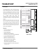
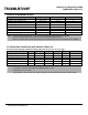
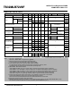
168PIN PC133 Registered DIMM
256MB With 32Mx8 CL3
Dimensions
Side Millimeters Inches
A 133.35±0.40 5.250±0.016
B 65.67 2.585
C 23.49 0.925
D 8.89 0.350
E 15.80 0.622
F 19.80 0.780
G 29.21±0.20 1.150±0.008
H 1.27±0.10 0.050±0.004
(Refer Placement)
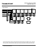
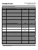
Pin Identification
Symbol Function
SA0~SA11
Address Input
SBA0, SBA1
Select Bank Address
SD0~SD63
Data Input / Output.
SCB0~SCB7
Check bit (data-in / data-out)
SCK0~SCK3
Clock Input.
SCKE0
Clock Enable Input.
/SCS0, SCS2
Chip Select Input.
/SRAS
Row Address Strobe
/SCAS
Column Address Strobe
/SWE
Write Enable
SDQM0~SDQM7
Data (DQ) Mask
SREGE
Register Enable
EA0~EA2
Address in EEPROM
SCL
Serial PD Clock
SDA
Serial PD Add/Data input/output
Vcc
+3.3 Voltage Power Supply
Vss
Ground
NC
No Connection
Transcend Information Inc. 2