
Datasheet

T
T
T
S
S
S
3
3
3
2
2
2
M
M
M
L
L
L
R
R
R
7
7
7
2
2
2
V
V
V
6
6
6
F
F
F
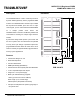
168PIN PC133 Registered DIMM
256MB With 32Mx8 CL3
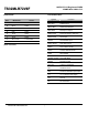
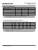
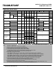
ABSOLUTE MAXIMUM RATINGS
Parameter Symbol Value Unit
Voltage on any pin relative to Vss VIN, VOUT -1.0~4.6 V
Voltage on VDD supply to Vss VDD, VDDQ -1.0~4.6 V
Storage temperature TSTG -55~+150 °C
Power dissipation PD 9 W
Short circuit current IOS 50 mA
Mean time between failure MTBF 50 year
Temperature Humidity Burning THB 85°C/85%, °C-%
Temperature Cycling Test TC 0°C ~ 125°C °C-Hr
Note:
Permanent device damage may occur if ABSOLUTE MAXIMUM RATINGS are exceeded.
Functional operation should be restricted to recommended operating condition.
Exposure to higher than recommended voltage for extended periods of time could affect device reliability.
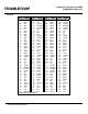
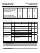
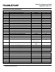
DC OPERATING CONDITIONS AND CHARACTERISTICS
Recommended operating conditions (Voltage referenced to Vss = 0V, TA = 0 to 70°C)
Parameter Symbol
Min
Typ Max Unit Note
Supply voltage VDD 3.0 3.3 3.6 V
Input high voltage VIH 2.0 3.0 VDD+0.3 V 1
Input low voltage VIL -0.3 0 0.8 V 2
Output high voltage VOH 2.4 - - V IOH=-2mA
Output low voltage VOL - - 0.4 V IOL=2mA
Input leakage current IIL -10 - 10 uA 3
Note:
1. VIH (max) = 5.6V AC .The overshoot voltage duration is ≤ 3ns.
2. VIL (min) = -2.0V AC .The undershoot voltage duration is ≤ 3ns.
3. Any input 0V ≤ VIN ≤ VDDQ.
Input leakage currents include Hi-Z output leakage for all bi-directional buffers with Tri-State outputs.
Transcend Information Inc. 5