
Datasheet

T
T
T
S
S
S
3
3
3
2
2
2
M
M
M
L
L
L
R
R
R
7
7
7
2
2
2
V
V
V
6
6
6
F
F
F
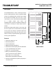
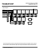
168PIN PC133 Registered DIMM
256MB With 32Mx8 CL3
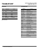
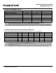
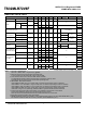
CAPACITANCE (VDD = 3.3V, TA = 23°C, f = 1MHz)
Parameter Symbol Min Max Unit
Input capacitance (SA0~SA11, SBA0~ SBA1)
Input capacitance (/SRAS, /SCAS, /SWE)
Input capacitance (SCKE0)
Input capacitance (SCLK0~SCLK3)
Input capacitance (/SCS0, /SCS2)
Input capacitance (SDQM0~SDQM7)
Data input/output capacitance (SD0~SD63)
Data input/output capacitance (SCB0~SCB7)
C
IN1
CIN2
CIN3
CIN4
CIN5
CIN6
COUT
COUT1
-
-
-
-
-
-
-
-
15
15
15
23
15
15
16
16
pF
pF
pF
pF
pF
pF
pF
pF
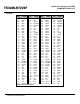
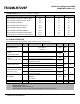
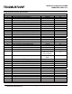
DC CHARACTERISTICS
(Recommended operating condition unless otherwise noted, TA = 0 to 70°C)
Parameter Symbol Test Condition CAS Latency Value Unit Note
Operating Current
(One Bank Active)
ICC1 Burst Length =1
t
RC≥tRC(min)
I
OL=0mA
1,630 mA 1
ICC2P CKE≤VIL(max), tCC=10ns 368 Precharge Standby
Current
in power-down mode
I
CC2PS
CKE & CLK≤V
IL(max), tCC=∞
20
mA 3
ICC2N CKE≥VIH(min), /CS≥VIH(min), tCC=10ns
Input signals are changed one time during 20ns
494
Precharge Standby
Current
in non power-down mode
I
CC2NS
CKE≥V
IH(min), CLK≤VIL(max), tCC=∞
Input signals are stable
128
mA
3
ICC3P CKE≤VIL(max), tCC=10ns
404
Active Standby Current
in power-down mode
I
CC3PS
CKE & CLK≤V
IL(max), tCC=∞
56
mA 3
ICC3N CKE≥VIH(min), /CS≥VIH(min), tCC=10ns
Input signals are changed one time during 20ns
620
Active Standby Current
in non power-down mode
(One Bank Active)
I
CC3NS
CKE≥V
IH(min), CLK≤VIL(max), tCC=∞
Input signals are stable
227
mA
3
Operating Current
(Bust Mode)
ICC4 IOL= 0 mA
Page Burst
tcc
D = 2CLKs
1,610 mA 1
Refresh Current ICC5 tRC≥tRC(min) 2,240 mA 2
Self Refresh Current ICC6 CKE≤0.2V 395 mA 3
Note:
1. Measured with outputs open.
2. Refresh period is 64ms.
3. Measured with 1 PLL & 2 Drive Ics
4. Unless otherwise noticed, input swing level is CMOS (VIH/\VIL=VDDQ/VSSQ)
Transcend Information Inc. 6