
Datasheet

T
T
T
S
S
S
3
3
3
2
2
2
M
M
M
L
L
L
R
R
R
7
7
7
2
2
2
V
V
V
6
6
6
F
F
F
168PIN PC133 Registered DIMM
256MB With 32Mx8 CL3
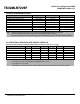
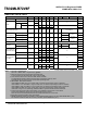
AC OPERATING TEST CONDITIONS (VDD = 3.3V±0.3V, TA = 0 to 70°C)
Parameter Value Unit
AC Input levels (VIH/VIL) 2.4/0.4 V
Input timing measurement reference level 1.4 V
Input rise and fall time tr/tf=1/1 ns
Output timing measurement reference level 1.4 V
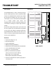
Output load condition See Fig. 2
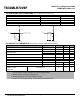
Output
(Fig. 1) DC Output Load Circuit
3.3V
1200 Ohm
50pF
870 Ohm
V
OH
(DC)=2.4V, I
OH
=-2mA
V
OL
(DC)=0.4V, I
OL
=2mA
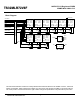
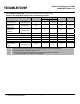
Output
(Fig. 2) AC Output Load Circuit
Vtt=1.4V
50 Ohm
50pF
Z0=50 Ohm
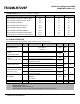
OPERATING AC PARAMETER (AC operating conditions unless otherwise noted)
Parameter Symbol Value Unit Note
/RAS to /CAS delay tRCD(min) 15 ns 1
Row precharge time tRP(min) 20 ns 1
tRAS(min) 45 ns 1
Row active time
tRAS(max) 100 us
Row cycle time tRC(min) 60 ns 1
Last data in to new col. address delay tCDL(min) 1 CLK 2
Last data in to row precharge tRDL(min) 2 CLK 2
Last data in to Active delay tDAL 2CLK+20ns
Last data in to burst stop tBDL(min) 1 CLK 2
Col. address to col. address delay tCCD(min) 1 CLK 3
Number of valid
output data
CAS latency=3 2
ea 4
Note:
1. The minimum number of clock cycles is determined by dividing the minimum time required with
clock cycle time, and then rounding off to the next higher integer.
2. Minimum delay is required to complete write.
3. All parts allow every cycle column address change.
4. In case of row precharge interrupt, auto precharge and read burst stop.
Transcend Information Inc. 7