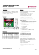
T Trraan nsscceen nd d IIn nd du ussttrriiaall C CF FC Caarrd d T TS S112288M M~~1166G GC CF F220000II Description Features The Transcend CF200I is a High Speed industrial • CompactFlash Specification Version 4.1 Compliant Compact Flash Card with high quality Flash Memory • RoHS compliant products assembled on a printed circuit board. • Single Power Supply: 3.
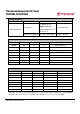
T Trraan nsscceen nd d IIn nd du ussttrriiaall C CF FC Caarrd d T TS S112288M M~~1166G GC CF F220000II Ordering Information Part Number Interface Transfer Mode Disk Type Ultra DMA mode 0~5 (UDMA4 as default) True IDE mode Fixed Disk (Default) Multi-Word DMA Mode 0~4 TS128M~16GCF200I PIO Mode 0 ~ 6 PC Card mode (PCMCIA) 80ns, 100ns, 120ns, 250ns Fixed Disk (Default) C.H.
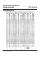
T Trraan nsscceen nd d IIn nd du ussttrriiaall C CF FC Caarrd d T TS S112288M M~~1166G GC CF F220000II Power Requirements (DC 5V @25℃) Power Consumption (mA) Part Number & Input Voltage TS128MCF200I TS256MCF200I TS512MCF200I TS1GCF200I TS2GCF200I TS4GCF200I TS8GCF200I TS16GCF200I Read Write 3.3V ± 10% 61 52.6 5V ± 10% 102.6 53.4 3.3V ± 10% 61.3 57.6 5V ± 10% 99 58.8 3.3V ± 10% 86.9 57.8 5V ± 10% 64.1 59.3 3.3V ± 10% 67.5 65.9 5V ± 10% 71.3 68.6 3.3V ± 10% 71 89.
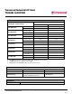
T Trraan nsscceen nd d IIn nd du ussttrriiaall C CF FC Caarrd d T TS S112288M M~~1166G GC CF F220000II More Functions to extend product life 1. Global Wear Leveling – Advanced algorithm to enhance the Wear-Leveling Efficiency There are 3 main processes in global wear leveling approaches: (1) Record the block erase count and save in the wear-leveling table. (2) Find the static-block and save it in wear-leveling pointer. (3) Check the erase count when the block popped from spare pool.
T Trraan nsscceen nd d IIn nd du ussttrriiaall C CF FC Caarrd d T TS S112288M M~~1166G GC CF F220000II Transcend Transcend Information Inc. 5 V1.
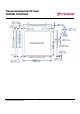
T Trraan nsscceen nd d IIn nd du ussttrriiaall C CF FC Caarrd d T TS S112288M M~~1166G GC CF F220000II Block Diagram Transcend Information Inc. 6 V1.
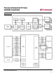
T Trraan nsscceen nd d IIn nd du ussttrriiaall C CF FC Caarrd d T TS S112288M M~~1166G GC CF F220000II Pin Assignments and Pin Type Transcend Information Inc. 7 V1.
T Trraan nsscceen nd d IIn nd du ussttrriiaall C CF FC Caarrd d T TS S112288M M~~1166G GC CF F220000II Note: 1) These signals are required only for 16 bit accesses and not required when installed in 8 bit systems. Devices should allow for 3-state signals not to consume current. 2) The signal should be grounded by the host. 3) The signal should be tied to VCC by the host. 4) The mode is required for CompactFlash Storage Cards. 5) The -CSEL signal is ignored by the card in PC Card modes.
T Trraan nsscceen nd d IIn nd du ussttrriiaall C CF FC Caarrd d T TS S112288M M~~1166G GC CF F220000II Signal Description Signal Name Dir.
T Trraan nsscceen nd d IIn nd du ussttrriiaall C CF FC Caarrd d T TS S112288M M~~1166G GC CF F220000II Signal Name Dir. Pin -CE1, -CE2 (PC Card Memory Mode) Card Enable I 7,32 Description These input signals are used both to select the card and to indicate to the card whether a byte or a word operation is being performed. -CE2 always accesses the odd byte of the word.-CE1 accesses the even byte or the Odd byte of the word depending on A0 and -CE2.
T Trraan nsscceen nd d IIn nd du ussttrriiaall C CF FC Caarrd d T TS S112288M M~~1166G GC CF F220000II Signal Name Dir. Pin -INPACK (PC Card Memory Mode) O 43 Description This signal is not used in this mode. -INPACK (PC Card I/O Mode) Input Acknowledge The Input Acknowledge signal is asserted by the CompactFlash Storage Card when the card is selected and responding to an I/O read cycle at the address that is on the address bus.
T Trraan nsscceen nd d IIn nd du ussttrriiaall C CF FC Caarrd d T TS S112288M M~~1166G GC CF F220000II Signal Name Dir. Pin -IOWR (PC Card Memory Mode) I 35 -IOWR (PC Card I/O Mode) Description This signal is not used in this mode. The I/O Write strobe pulse is used to clock I/O data on the Card Data bus into the CompactFlash Storage Card controller registers when the CompactFlash Storage Card is configured to use the I/O interface.
T Trraan nsscceen nd d IIn nd du ussttrriiaall C CF FC Caarrd d T TS S112288M M~~1166G GC CF F220000II Signal Name Dir. Pin -REG (PC Card Memory Mode) Attribute Memory Select I 44 Description This signal is used during Memory Cycles to distinguish between Common Memory and Register (Attribute) Memory accesses. High for Common Memory, Low for Attribute Memory. -REG (PC Card I/O Mode) The signal shall also be active (low) during I/O Cycles when the I/O address is on the Bus.
T Trraan nsscceen nd d IIn nd du ussttrriiaall C CF FC Caarrd d T TS S112288M M~~1166G GC CF F220000II Signal Name Dir. Pin -VS1 -VS2 (PC Card Memory Mode) O 33 40 Description Voltage Sense Signals. -VS1 is grounded on the Card and sensed by the Host so that the CompactFlash Storage Card CIS can be read at 3.3 volts and -VS2 is reserved by PCMCIA for a secondary voltage and is not connected on the Card. -VS1 -VS2 (PC Card I/O Mode) This signal is the same for all modes.
T Trraan nsscceen nd d IIn nd du ussttrriiaall C CF FC Caarrd d T TS S112288M M~~1166G GC CF F220000II Electrical Specification The following tables indicate all D.C. Characteristics for the CompactFlash Storage Card. Unless otherwise stated, conditions are: Vcc = 5V ±10% Vcc = 3.3V ± 5% Absolute Maximum Conditions Input Power Input Leakage Current Input Characteristics CompactFlash interface I/O at 5.0V Parameter Symbol Min. Max. 5.5 Supply Voltage VCC 4.
T Trraan nsscceen nd d IIn nd du ussttrriiaall C CF FC Caarrd d T TS S112288M M~~1166G GC CF F220000II CompactFlash interface I/O at 3.3V Parameter Symbol Min. Max. Unit 3.63 V Supply Voltage VCC 2.97 High level output voltage VOH VCC-0.8 Low level output voltage VOL High level input voltage VIH Low level input voltage VIL Pull up resistance 2 Pull down resistance Remark V 0.8 V 2.4 V Non-schmitt trigger 2.05 V Schmitt trigger 0.6 V Non-schmitt trigger 1.
T Trraan nsscceen nd d IIn nd du ussttrriiaall C CF FC Caarrd d T TS S112288M M~~1166G GC CF F220000II Output Drive Type Output Drive Characteristics Transcend Information Inc. 17 V1.
T Trraan nsscceen nd d IIn nd du ussttrriiaall C CF FC Caarrd d T TS S112288M M~~1166G GC CF F220000II Signal Interface Transcend Information Inc. 18 V1.
T Trraan nsscceen nd d IIn nd du ussttrriiaall C CF FC Caarrd d T TS S112288M M~~1166G GC CF F220000II Notes: 1) Control Signals: each card shall present a load to the socket no larger than 50 pF 10 at a DC current of 700 μ A low state and 150 μ A high state, including pull-resistor.
T Trraan nsscceen nd d IIn nd du ussttrriiaall C CF FC Caarrd d T TS S112288M M~~1166G GC CF F220000II Ultra DMA Electrical Requirements Host and Card signal capacitance limits for Ultra DMA operation The host interface signal capacitance at the host connector shall be a maximum of 25 pF for each signal as measured at 1 MHz. The card interface signal capacitance at the card connector shall be a maximum of 20 pF for each signal as measured at 1 MHz.
T Trraan nsscceen nd d IIn nd du ussttrriiaall C CF FC Caarrd d T TS S112288M M~~1166G GC CF F220000II Table: Ultra DMA Termination with Pull-up or Pull down Example Printed Circuit Board (PCB) Trace Requirements for Ultra DMA On any PCB for a host or device supporting Ultra DMA: The longest D[15:00] trace shall be no more than 0.5" longer than either STROBE trace as measured from the IC pin to the connector. The shortest D[15:00] trace shall be no more than 0.
T Trraan nsscceen nd d IIn nd du ussttrriiaall C CF FC Caarrd d T TS S112288M M~~1166G GC CF F220000II Attribute Memory Read Timing Specification Transcend Information Inc. 22 V1.
T Trraan nsscceen nd d IIn nd du ussttrriiaall C CF FC Caarrd d T TS S112288M M~~1166G GC CF F220000II Configuration Register (Attribute Memory) Write Timing Specification Transcend Information Inc. 23 V1.
T Trraan nsscceen nd d IIn nd du ussttrriiaall C CF FC Caarrd d T TS S112288M M~~1166G GC CF F220000II Common Memory Read Timing Specification Transcend Information Inc. 24 V1.
T Trraan nsscceen nd d IIn nd du ussttrriiaall C CF FC Caarrd d T TS S112288M M~~1166G GC CF F220000II Common Memory Write Timing Specification Transcend Information Inc. 25 V1.
T Trraan nsscceen nd d IIn nd du ussttrriiaall C CF FC Caarrd d T TS S112288M M~~1166G GC CF F220000II I/O Input (Read) Timing Specification Transcend Information Inc. 26 V1.
T Trraan nsscceen nd d IIn nd du ussttrriiaall C CF FC Caarrd d T TS S112288M M~~1166G GC CF F220000II I/O Output (Write) Timing Specification Transcend Information Inc. 27 V1.
T Trraan nsscceen nd d IIn nd du ussttrriiaall C CF FC Caarrd d T TS S112288M M~~1166G GC CF F220000II Transcend Information Inc. 28 V1.
T Trraan nsscceen nd d IIn nd du ussttrriiaall C CF FC Caarrd d T TS S112288M M~~1166G GC CF F220000II True IDE PIO Mode Read/Write Timing Specification Transcend Information Inc. 29 V1.
T Trraan nsscceen nd d IIn nd du ussttrriiaall C CF FC Caarrd d T TS S112288M M~~1166G GC CF F220000II Transcend Information Inc. 30 V1.
T Trraan nsscceen nd d IIn nd du ussttrriiaall C CF FC Caarrd d T TS S112288M M~~1166G GC CF F220000II Transcend Information Inc. 31 V1.
T Trraan nsscceen nd d IIn nd du ussttrriiaall C CF FC Caarrd d T TS S112288M M~~1166G GC CF F220000II True IDE Ultra DMA Mode Read/Write Timing Specification Table: Ultra DMA Data Burst Timing Transcend Information Inc. 32 V1.
T Trraan nsscceen nd d IIn nd du ussttrriiaall C CF FC Caarrd d T TS S112288M M~~1166G GC CF F220000II Notes: 1) All timing measurement switching points (low to high and high to low) shall be taken at 1.5 V. 2) All signal transitions for a timing parameter shall be measured at the connector specified in the measurement location column. For example, in the case of tRFS, both STROBE and –DMARDY transitions are measured at the sender connector.
T Trraan nsscceen nd d IIn nd du ussttrriiaall C CF FC Caarrd d T TS S112288M M~~1166G GC CF F220000II Transcend Information Inc. 34 V1.
T Trraan nsscceen nd d IIn nd du ussttrriiaall C CF FC Caarrd d T TS S112288M M~~1166G GC CF F220000II Notes: 1) The parameters tUI, tMLI : (Ultra DMA Data-In Burst Device Termination Timing and Ultra DMA Data-In Burst Host Termination Timing), and tLI indicate sender-to-recipient or recipient-to-sender interlocks, i.e., one agent (either sender or recipient) is waiting for the other agent to respond with a signal before proceeding. tUI is an unlimited interlock that has no maximum time value.
T Trraan nsscceen nd d IIn nd du ussttrriiaall C CF FC Caarrd d T TS S112288M M~~1166G GC CF F220000II Table: Ultra DMA Sender and Recipient IC Timing Requirements Note: 1) The sender shall be tested while driving an 18 inch long, 80 conductor cable with PVC insulation material. The signal under test shall be cut at a test point so that it has not trace, cable or recipient loading after the test point. All other signals should remain connected through to the recipient.
T Trraan nsscceen nd d IIn nd du ussttrriiaall C CF FC Caarrd d T TS S112288M M~~1166G GC CF F220000II Card Configuration The CompactFlash Storage Cards is identified by appropriate information in the Card Information Structure (CIS). The following configuration registers are used to coordinate the I/O spaces and the Interrupt level of cards that are located in the system.
T Trraan nsscceen nd d IIn nd du ussttrriiaall C CF FC Caarrd d T TS S112288M M~~1166G GC CF F220000II Attribute Memory Function Attribute memory is a space where CompactFlash Storage Card identification and configuration information are stored, and is limited to 8 bit wide accesses only at even addresses. The card configuration registers are also located here. For CompactFlash Storage Cards, the base address of the ard configuration registers is 200h.
T Trraan nsscceen nd d IIn nd du ussttrriiaall C CF FC Caarrd d T TS S112288M M~~1166G GC CF F220000II Configuration Option Register (Base + 00h in Attribute Memory) Transcend Information Inc. 39 V1.
T Trraan nsscceen nd d IIn nd du ussttrriiaall C CF FC Caarrd d T TS S112288M M~~1166G GC CF F220000II Card Configuration and Status Register (Base + 02h in Attribute Memory) Transcend Information Inc. 40 V1.
T Trraan nsscceen nd d IIn nd du ussttrriiaall C CF FC Caarrd d T TS S112288M M~~1166G GC CF F220000II Pin Replacement Register (Base + 04h in Attribute Memory) Transcend Information Inc. 41 V1.
T Trraan nsscceen nd d IIn nd du ussttrriiaall C CF FC Caarrd d T TS S112288M M~~1166G GC CF F220000II Socket and Copy Register (Base + 06h in Attribute Memory) Transcend Information Inc. 42 V1.
T Trraan nsscceen nd d IIn nd du ussttrriiaall C CF FC Caarrd d T TS S112288M M~~1166G GC CF F220000II I/O Transfer Function The I/O transfer to or from the CompactFlash Storage can be either 8 or 16 bits. When a 16 bit accessible port is addressed, the signal -IOIS16 is asserted by the CompactFlash Storage. Otherwise, the -IOIS16 signal is de-asserted.
T Trraan nsscceen nd d IIn nd du ussttrriiaall C CF FC Caarrd d T TS S112288M M~~1166G GC CF F220000II Common Memory Transfer Function The Common Memory transfer to or from the CompactFlash Storage can be either 8 or 16 bits. Table: Common Memory Function Transcend Information Inc. 44 V1.
T Trraan nsscceen nd d IIn nd du ussttrriiaall C CF FC Caarrd d T TS S112288M M~~1166G GC CF F220000II True IDE Mode I/O Transfer Function The CompactFlash Storage Card can be configured in a True IDE Mode of operation. The CompactFlash Storage Card is configured in this mode only when the -OE input signal is grounded by the host during the power off to power on cycle. Optionally, CompactFlash Storage Cards may support the following optional detection methods: 1.
T Trraan nsscceen nd d IIn nd du ussttrriiaall C CF FC Caarrd d T TS S112288M M~~1166G GC CF F220000II Metaformat Overview The goal of the Metaformat is to describe the requirements and capabilities of the CompactFlash Storage Card as thoroughly as possible. This includes describing the power requirements, IO requirements, memory requirements, manufacturer information and details about the services provided.
T Trraan nsscceen nd d IIn nd du ussttrriiaall C CF FC Caarrd d T TS S112288M M~~1166G GC CF F220000II CF-ATA Drive Register Set Definition and Protocol The CompactFlash Storage Card can be configured as a high performance I/O device through: a) The standard PC-AT disk I/O address spaces 1F0h-1F7h, 3F6h-3F7h (primary) or 170h- 177h, 376h-377h (secondary) with IRQ 14 (or other available IRQ). b) Any system decoded 16 byte I/O block using any available IRQ. c) Memory space.
T Trraan nsscceen nd d IIn nd du ussttrriiaall C CF FC Caarrd d T TS S112288M M~~1166G GC CF F220000II I/O Primary and Secondary Address Configurations Table: Primary and Secondary I/O Decoding Transcend Information Inc. 48 V1.
T Trraan nsscceen nd d IIn nd du ussttrriiaall C CF FC Caarrd d T TS S112288M M~~1166G GC CF F220000II Contiguous I/O Mapped Addressing When the system decodes a contiguous block of I/O registers to select the CompactFlash Storage Card, the registers are accessed in the block of I/O space decoded by the system as follows: Table: Contiguous I/O Decoding Transcend Information Inc. 49 V1.
T Trraan nsscceen nd d IIn nd du ussttrriiaall C CF FC Caarrd d T TS S112288M M~~1166G GC CF F220000II Memory Mapped Addressing When the CompactFlash Storage Card registers are accessed via memory references, the registers appear in the common memory space window: 0-2K bytes as follows: True IDE Mode Addressing When the CompactFlash Storage Card is configured in the True IDE Mode, the I/O decoding is as follows: Transcend Information Inc. 50 V1.
T Trraan nsscceen nd d IIn nd du ussttrriiaall C CF FC Caarrd d T TS S112288M M~~1166G GC CF F220000II CF-ATA Registers The following section describes the hardware registers used by the host software to issue commands to the CompactFlash device. These registers are often collectively referred to as the “task file.
T Trraan nsscceen nd d IIn nd du ussttrriiaall C CF FC Caarrd d T TS S112288M M~~1166G GC CF F220000II Feature Register (Address - 1F1h[171h]; Offset 1, 0Dh Write Only) This register provides information regarding features of the CompactFlash Storage Card that the host can utilize. This register is also accessed in PC Card modes on data bits D15-D8 during a write operation to Offset 0 with -CE2 low and -CE1 high.
T Trraan nsscceen nd d IIn nd du ussttrriiaall C CF FC Caarrd d T TS S112288M M~~1166G GC CF F220000II Bit 3 (HS3): when operating in the Cylinder, Head, Sector mode, this is bit 3 of the head number. It is Bit 27 in the Logical Block Address mode. Bit 2 (HS2): when operating in the Cylinder, Head, Sector mode, this is bit 2 of the head number. It is Bit 26 in the Logical Block Address mode. Bit 1 (HS1): when operating in the Cylinder, Head, Sector mode, this is bit 1 of the head number.
T Trraan nsscceen nd d IIn nd du ussttrriiaall C CF FC Caarrd d T TS S112288M M~~1166G GC CF F220000II Device Control Register (Address - 3F6h[376h]; Offset Eh) This register is used to control the CompactFlash Storage Card interrupt request and to issue an ATA soft reset to the card. This register can be written even if the device is BUSY. The bits are defined as follows: Bit 7: this bit is ignored by the CompactFlash Storage Card. The host software should set this bit to 0.
T Trraan nsscceen nd d IIn nd du ussttrriiaall C CF FC Caarrd d T TS S112288M M~~1166G GC CF F220000II Card (Drive) Address Register (Address 3F7h[377h]; Offset Fh) This register is provided for compatibility with the AT disk drive interface. It is recommended that this register not be mapped into the host’s I/O space because of potential conflicts on Bit 7. Bit 7: this bit is unknown.
T Trraan nsscceen nd d IIn nd du ussttrriiaall C CF FC Caarrd d T TS S112288M M~~1166G GC CF F220000II CF-ATA Command Set Transcend Information Inc. 56 V1.
T Trraan nsscceen nd d IIn nd du ussttrriiaall C CF FC Caarrd d T TS S112288M M~~1166G GC CF F220000II Transcend Information Inc. 57 V1.
T Trraan nsscceen nd d IIn nd du ussttrriiaall C CF FC Caarrd d T TS S112288M M~~1166G GC CF F220000II Request Sense - 03h The extended error code is returned to the host in the Error Register. Write Sector(s) without Erase - 38h Transcend Information Inc. 58 V1.
T Trraan nsscceen nd d IIn nd du ussttrriiaall C CF FC Caarrd d T TS S112288M M~~1166G GC CF F220000II Erase Sector(s) - C0h This command is used to pre-erase and condition data sectors in advance of a Write without Erase or Write Multiple without Erase command. There is no data transfer associated with this command but a Write Fault error status can occur. Write Multiple without Erase – CDh Translate Sector - 87h Transcend Information Inc. 59 V1.
T Trraan nsscceen nd d IIn nd du ussttrriiaall C CF FC Caarrd d T TS S112288M M~~1166G GC CF F220000II Translate Sector Information Transcend Information Inc. 60 V1.
T Trraan nsscceen nd d IIn nd du ussttrriiaall C CF FC Caarrd d T TS S112288M M~~1166G GC CF F220000II Set Features – EFh Feature Supported Feature 03h 81h 82h Operation Set transfer mode based on calue in Sector Count register Disable 8 bit data transfer Disable Write Cache Execute Drive Diagnostic - 90h When the diagnostic command is issued in a PCMCIA configuration mode, this command runs only on the CompactFlash Storage Card that is addressed by the Drive/Head register.
T Trraan nsscceen nd d IIn nd du ussttrriiaall C CF FC Caarrd d T TS S112288M M~~1166G GC CF F220000II Transcend Information Inc. 62 V1.
T Trraan nsscceen nd d IIn nd du ussttrriiaall C CF FC Caarrd d T TS S112288M M~~1166G GC CF F220000II Flush Cache – E7h This command causes the card to complete writing data from its cache. The card returns status with RDY=1 and DSC=1 after the data in the write cache buffer is written to the media. If the Compact Flash Storage Card does not support the Flush Cache command, the Compact Flash Storage Card shall return command aborted.
T Trraan nsscceen nd d IIn nd du ussttrriiaall C CF FC Caarrd d T TS S112288M M~~1166G GC CF F220000II Read Sector(s) - 20h or 21h Read Verify Sector(s) - 40h or 41h Set Multiple Mode - C6h Write DMA – CAh Transcend Information Inc. 64 V1.
T Trraan nsscceen nd d IIn nd du ussttrriiaall C CF FC Caarrd d T TS S112288M M~~1166G GC CF F220000II Write Multiple Command - C5h Write Sector(s) - 30h or 31h NOP - 00h This command always fails with the CompactFlash Storage Card returning command aborted. Transcend Information Inc. 65 V1.
T Trraan nsscceen nd d IIn nd du ussttrriiaall C CF FC Caarrd d T TS S112288M M~~1166G GC CF F220000II Read Buffer - E4h The Read Buffer command enables the host to read the current contents of the CompactFlash Storage Card’s sector buffer. This command has the same protocol as the Read Sector(s) command. Write Buffer - E8h Check Power Mode - 98h or E5h If the CompactFlash Storage Card is in, going to, or recovering from the sleep mode, the CompactFlash Storage Transcend Information Inc.
T Trraan nsscceen nd d IIn nd du ussttrriiaall C CF FC Caarrd d T TS S112288M M~~1166G GC CF F220000II Card sets BSY, sets the Sector Count Register to 00h, clears BSY and generates an interrupt. If the CompactFlash Storage Card is in Idle mode, the CompactFlash Storage Card sets BSY, sets the Sector Count Register to FFh, clears BSY and generates an interrupt. Idle - 97h or E3h This command causes the CompactFlash Storage Card to set BSY, enter the Idle mode, clear BSY and generate an interrupt.
T Trraan nsscceen nd d IIn nd du ussttrriiaall C CF FC Caarrd d T TS S112288M M~~1166G GC CF F220000II Standby - 96h or E2h Standby Immediate - 94h or E0h Security Set Password – F1h Transcend Information Inc. 68 V1.
T Trraan nsscceen nd d IIn nd du ussttrriiaall C CF FC Caarrd d T TS S112288M M~~1166G GC CF F220000II Table Security Unlock – F2h Security Erase Prepare – F3h Transcend Information Inc. 69 V1.
T Trraan nsscceen nd d IIn nd du ussttrriiaall C CF FC Caarrd d T TS S112288M M~~1166G GC CF F220000II Security Erase Unit – F4h Security Freeze Lock – F5h Transcend Information Inc. 70 V1.
T Trraan nsscceen nd d IIn nd du ussttrriiaall C CF FC Caarrd d T TS S112288M M~~1166G GC CF F220000II Security Freeze Lock – F6h Format Track - 50h This command writes the desired head and cylinder of the selected drive with a vendor unique data pattern (typically FFh or 00h).
T Trraan nsscceen nd d IIn nd du ussttrriiaall C CF FC Caarrd d T TS S112288M M~~1166G GC CF F220000II Seek - 7Xh Wear Level - F5h Write Verify - 3Ch Error Posting Transcend Information Inc. 72 V1.
T Trraan nsscceen nd d IIn nd du ussttrriiaall C CF FC Caarrd d T TS S112288M M~~1166G GC CF F220000II Transcend Information Inc. 73 V1.
T Trraan nsscceen nd d IIn nd du ussttrriiaall C CF FC Caarrd d T TS S112288M M~~1166G GC CF F220000II Error and Status Register summarizes the valid status and error value for all the CF-ATA Command set. Transcend Information Inc. 74 V1.
T Trraan nsscceen nd d IIn nd du ussttrriiaall C CF FC Caarrd d T TS S112288M M~~1166G GC CF F220000II ID Table Information of True IDE Mode Word Address Default Value Total Bytes Data Field Type Information 044Ah 2 General configuration - signature for the CompactFlash Flash Storage Card 0XXX 2 General configuration – Bit Significant with ATA-4 definitions.
T Trraan nsscceen nd d IIn nd du ussttrriiaall C CF FC Caarrd d T TS S112288M M~~1166G GC CF F220000II Word Address Default Value Total Bytes 67 0078h 2 Minimum PIO transfer cycle time without flow control 68 0078h 2 Minimum PIO transfer cycle time with IORDY flow control 69-79 0000h 20 Reserved 80-81 0000h 4 Reserved – CF cards do not return an ATA version 82-84 702Bh 2 Command sets supported 83 500Ch 2 Command sets supported Data Field Type Information 84 4000h 2 Command
T Trraan nsscceen nd d IIn nd du ussttrriiaall C CF FC Caarrd d T TS S112288M M~~1166G GC CF F220000II Removable Device while preserving all Retired bits in the word. 0040h: This is the alternate value of Word 0 turns on ATA device and turns off Removable Media and Removable Device while zeroing all Retired bits in the word Bit 15-12: Configuration Flag If bits 15:12 are set to 8h then Word 0 shall be 848Ah.
T Trraan nsscceen nd d IIn nd du ussttrriiaall C CF FC Caarrd d T TS S112288M M~~1166G GC CF F220000II This field contains the model number for this product and is left justified and padded with spaces (20h). Word 47: Read/Write Multiple Sector Count Bits 15-8 shall be the recommended value of 80h or the permitted value of 00h. Bits 7-0 of this word define the maximum number of sectors per block that the CompactFlash Storage Card supports for Read/Write Multiple commands.
T Trraan nsscceen nd d IIn nd du ussttrriiaall C CF FC Caarrd d T TS S112288M M~~1166G GC CF F220000II indicates that Multiword DMA mode 0 has been selected. Bit 9, if set to one, indicates that Multiword DMA mode 1 has been selected. Bit 10, if set to one, indicates that Multiword DMA mode 2 has been selected. Selection of Multiword DMA modes 3 and above are specific to CompactFlash are reported in word 163, Word 163: CF Advanced True IDE Timing Mode Capabilities and Settings.
T Trraan nsscceen nd d IIn nd du ussttrriiaall C CF FC Caarrd d T TS S112288M M~~1166G GC CF F220000II Word 68: Minimum PIO transfer cycle time with IORDY Word 68 of the parameter information of the Identify Device command is defined as the minimum PIO transfer with IORDY flow control cycle time. This field defines, in nanoseconds, the minimum cycle time that the CompactFlash Storage Card supports while performing data transfers while utilizing IORDY flow control.
T Trraan nsscceen nd d IIn nd du ussttrriiaall C CF FC Caarrd d T TS S112288M M~~1166G GC CF F220000II Bit 0 of word 85 shall be set to zero; the SMART feature set is not enabled. If bit 1 of word 85 is set to one, the Security Mode feature set has been enabled via the Security Set Password command. Bit 2 of word 85 shall be set to zero; the Removable Media feature set is not supported. Bit 3 of word 85 shall be set to one; the Power Management feature set is supported.
T Trraan nsscceen nd d IIn nd du ussttrriiaall C CF FC Caarrd d T TS S112288M M~~1166G GC CF F220000II Word 90: Time required for Enhanced security erase unit completion Word 90 specifies the time required for the Enhanced Security Erase Unit command to complete. This command shall be supported on CompactFlash Storage Cards that support security.
T Trraan nsscceen nd d IIn nd du ussttrriiaall C CF FC Caarrd d T TS S112288M M~~1166G GC CF F220000II Word 163: CF Advanced True IDE Timing Mode Capabilities and Settings This word describes the capabilities and current settings for CFA defined advanced timing modes using the True IDE interface. Notice! The use of True IDE PIO Modes 5 and above or of Multiword DMA Modes 3 and above impose significant restrictions on the implementation of the host: Additional Requirements for CF Advanced Timing Modes.
T Trraan nsscceen nd d IIn nd du ussttrriiaall C CF FC Caarrd d T TS S112288M M~~1166G GC CF F220000II Bits 2-0: Maximum Advanced PCMCIA I/O Mode Support Indicates the maximum I/O timing mode supported by the card. Value 0 1 2 3 4-7 Maximum PCMCIA IO timing mode Supported 255ns Cycle PCMCIA I/O Mode 120ns Cycle PCMCIA I/O Mode 100ns Cycle PCMCIA I/O Mode 80ns Cycle PCMCIA I/O Mode Reserved Bits 5-3: Maximum Memory timing mode supported Indicates the Maximum Memory timing mode supported by the card.
T Trraan nsscceen nd d IIn nd du ussttrriiaall C CF FC Caarrd d T TS S112288M M~~1166G GC CF F220000II SMART Command Set SMART Command Set SMART Feature Register Values D0h Read Data D5h Read Log D1h Read Attribute Threshold D6h Write Log D2h Enable/Disable Autosave D8h Enable SMART Operations D3h Save Attribute Values D9h Disable SMART Operations D4h Execute OFF-LINE Immediate DAh Return Status 1.
T Trraan nsscceen nd d IIn nd du ussttrriiaall C CF FC Caarrd d T TS S112288M M~~1166G GC CF F220000II 398-399 V Number of run time bad block (398=MSB, 399=LSB) 400 V Number of spare block 401-402 V Erase count (Low word) 403-405 F ‘SMI’ 406 F Number of max pair 407-410 V Erase Count (407-408=High word, 409-410=Low word) 411-510 X Vendor specific 511 V Data structure checksum F=the content of the byte is fixed and does not change.
T Trraan nsscceen nd d IIn nd du ussttrriiaall C CF FC Caarrd d T TS S112288M M~~1166G GC CF F220000II Ordering Information TS XG CF200I Transcend Product Capacity: 128M-512M = 128 MB up to 512 MB 1G-16G = 1 GB up to 16 GB Extreme Industrial CF card 1. The above technical information is based on industry standard data and has been tested to be reliable.