
Datasheet

TMC2041 DATASHEET (Rev. 1.02 / 2017-MAY-16) 55
www.trinamic.com
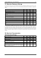
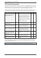
17 Absolute Maximum Ratings
The maximum ratings may not be exceeded under any circumstances. Operating the circuit at or near
more than one maximum rating at a time for extended periods shall be avoided by application
design.
Parameter
Symbol
Min
Max
Unit
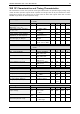
Supply voltage operating with inductive load (V
VS
≥ V
VSA
)
V
VS
, V
VSA
-0.5
27
V
Supply and bridge voltage max. *)
V
VS
-0.5
28
V
VSA when different from to VS
V
VSA
-0.5
V
VS
+0.5
V
I/O supply voltage
V
VIO
-0.5
5.5
V
digital VCC supply voltage (if not supplied by internal
regulator)
V
VCC
-0.5
5.5
V
Logic input voltage
V
I
-0.5
V
VIO
+0.5
V
Maximum current to / from digital pins
and analog low voltage I/Os
I
IO
+/-10
mA
5V regulator output current (internal plus external load)
I
5VOUT
50
mA
5V regulator continuous power dissipation (V
VM
-5V) * I
5VOUT
P
5VOUT
1
W
Power bridge repetitive output current
I
Ox
2.0
A
Junction temperature
T
J
-50
150
°C
Storage temperature
T
STG
-55
150
°C
ESD-Protection for interface pins (Human body model,
HBM)
V
ESDAP
4 (tbd.)
kV
ESD-Protection for handling (Human body model, HBM)
V
ESD
1 (tbd.)
kV
*) Stray inductivity of GND and VS connections will lead to ringing of the supply voltage when driving
an inductive load. This ringing results from the fast switching slopes of the driver outputs in
combination with reverse recovery of the body diodes of the output driver MOSFETs. Even small trace
inductivities as well as stray inductivity of sense resistors can easily generate a few volts of ringing
leading to temporary voltage overshoot. This should be considered when working near the maximum
voltage.
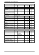
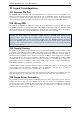
18 Electrical Characteristics
18.1 Operational Range
Parameter
Symbol
Min
Max
Unit
Junction temperature
T
J
-40
125
°C
Supply voltage (using internal +5V regulator)
V
VS
5.5
26
V
Supply voltage (internal +5V regulator bridged: V
VCC
=V
VSA
)
V
VS
4.7
5.4
V
I/O supply voltage
V
VIO
3.00
5.25
V
VCC voltage when using optional external source (supplies
digital logic and charge pump)
V
VCC
4.6
5.25
V
RMS motor coil current per coil (value for design guideline)
I
RMS
0.8
A
Peak output current per motor coil output (sine wave peak)
I
Ox
1.1
A
Peak output current per motor coil output (sine wave peak)
Limit T
J
≤ 105°C, e.g. for 100ms short time acceleration
phase below 50% duty cycle.
I
Ox
1.5
A