
Datasheet

TMC6200 DATASHEET (Rev. 1.04 / 2019-AUG-08) 35
www.trinamic.com
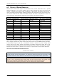
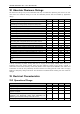
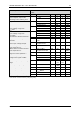
10 Absolute Maximum Ratings
The maximum ratings may not be exceeded under any circumstances. Operating the circuit at or near
more than one maximum rating at a time for extended periods shall be avoided by application
design.
Parameter
Symbol
Min
Max
Unit
Supply voltage operating with inductive load
V
VS
, V
VSA
-0.5
65
V
Supply and bridge voltage short time peak (limited by
peak voltage on charge pump output and Cxx pins*)
V
VSMAX
70
V
VSA supply voltage
V
VSAMAX
-0.5
65
V
Peak voltages on Cxx bootstrap pins and VCP
V
CxCP
85
V
Supply voltage V12
V
12VOUT
-0.5
15
V
Peak voltages on U/V/W pins (due to stray inductivity)
V
X
-6
V
VS
+6
V
Peak voltages on Cxx bootstrap pins relative to BM
V
Cxx
-0.5
16
V
I/O supply voltage
V
VIO
-0.5
5.5
V
Supply voltage (5VOUT)
V
5VOUT
-0.5
5.5
V
Logic input voltage
V
I
-0.5
V
VIO
+0.5
V
Maximum current to / from digital pins
and analog low voltage I/Os (short time peak current)
I
IO
+/-500
mA
Maximum differential input voltage for current amplifier
V
X
-V
SENSEX
+/-1.5
V
Maximum short time input current for current amplifier
I
SENSEX
+/-200
mA
5V regulator output current (internal plus external load)
I
5VOUT
30
mA
5V regulator continuous power dissipation (V
VSA
-5V) * I
5VOUT
P
5VOUT
1
W
12V regulator output current (internal plus external load)
I
12VOUT
20
mA
12V regulator continuous power dissipation (V
VM
-5V) * I
5VOUT
P
12VOUT
0.5
W
Junction temperature
T
J
-50
150
°C
Storage temperature
T
STG
-55
150
°C
ESD-Protection for interface pins (Human body model,
HBM)
V
ESDAP
4
kV
ESD-Protection for handling (Human body model, HBM)
V
ESD
1
kV
*) Stray inductivity of power routing will lead to ringing of the supply voltage when driving an
inductive load. This ringing results from the fast switching slopes of the driver outputs in
combination with reverse recovery of the body diodes of the output driver MOSFETs. Even small trace
inductivities as well as stray inductivity of sense resistors can easily generate a few volts of ringing
leading to temporary voltage overshoot. This should be considered when working near the maximum
voltage.
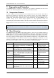
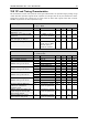
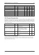
11 Electrical Characteristics
11.1 Operational Range
Parameter
Symbol
Min
Max
Unit
Junction temperature
T
J
-40
125
°C
Supply voltage for motor and bridge
V
VS
10
60
V
Supply voltage VSA
V
VSA
10
60
V
Supply voltage for VSA and 12OUT (internal gate voltage
regulator bridged)
V
12VOUT
,
V
VSA
10
13
V
Lower Supply voltage (reduced spec, short to GND
protection not functional), lower limit depending on
MOSFETs gate threshold voltage and load current
V
VS
8
V
I/O supply voltage
V
VIO
3.00
5.25
V