
Datasheet

TMC6200 DATASHEET (Rev. 1.04 / 2019-AUG-08) 36
www.trinamic.com
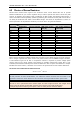
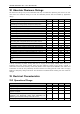
11.2 DC and Timing Characteristics
DC characteristics contain the spread of values guaranteed within the specified supply voltage range
unless otherwise specified. Typical values represent the average value of all parts measured at +25°C.
Temperature variation also causes stray to some values. A device with typical values will not leave
Min/Max range within the full temperature range.
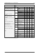
Power Supply Current
DC-Characteristics
V
VS
= V
VSA
= 24.0V
Parameter
Symbol
Conditions
Min
Typ
Max
Unit
Total supply current, driver
disabled I
VS
+ I
VSA
I
S
internal clock
11
15
mA
VSA supply current (VS and VSA
separated)
I
VSA
f
CLK
=24MHz / internal
clock, driver disabled
8
mA
Internal current consumption
from 5V supply on VCC pin
I
VCC
f
CLK
=24MHz
6
mA
IO supply current (typ. at 5V)
I
VIO
no load on outputs,
inputs at V
IO
or GND
Excludes pullup /
pull-down resistors
15
30
µA
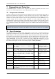
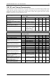
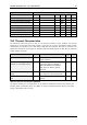
Motor Driver
DC- and Timing-Characteristics
V
VS
= 24.0V; Tj=50°C
Parameter
Symbol
Conditions
Min
Typ
Max
Unit
RDS
ON
lowside off driver
R
ONL
Gate off
1.0
1.6
Ω
RDS
ON
highside off driver
R
ONH
Gate off
1.3
2.0
Ω
Gate drive current low side
MOSFET turning on at 2V V
GS
I
SLPON0
DRIVESTRENGTH=0
400
mA
I
SLPON2
DRIVESTRENGTH=2
800
mA
I
SLPON3
DRIVESTRENGTH=3
1200
mA
Gate drive current high side
MOSFET turning on at 2V V
GS
I
SLPON0
DRIVESTRENGTH=0
400
mA
I
SLPON2
DRIVESTRENGTH=2
800
mA
I
SLPON3
DRIVESTRENGTH=3
1200
mA
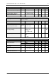
Gate drive current low side
MOSFET turning off at 4V V
GS
I
SLPOFF0
DRIVESTRENGTH=0
600
mA
I
SLPOFF2
DRIVESTRENGTH=2
1200
mA
I
SLPOFF3
DRIVESTRENGTH=3
1800
mA
Gate drive current high side
MOSFET turning on at 4V V
GS
I
SLPOFF0
DRIVESTRENGTH=0
600
mA
I
SLPOFF2
DRIVESTRENGTH=2
1200
mA
I
SLPOFFN3
DRIVESTRENGTH=3
1800
mA
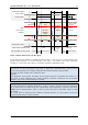
Minimum effective BBM time
enforced in individual or
singleline mode
t
BBM0
Individual LS and HS
signals (singleline=0)
30
50
70
ns
Reaction delay time LS/HS input
signal change to start of gate
driver output change
t
DLY
Individual LS and HS
signals (singleline=0)
65
85
110
ns
Matching difference of gate
driver reaction delay times
t
DLYMATCH
Individual LS and HS
signals (singleline=0)
10
ns