S8236 Version 1.0 Copyright Copyright © 2010 MiTAC International Corporation. All rights reserved. No part of this manual may be reproduced or translated without prior written consent from MiTAC International Corporation. Trademark All registered and unregistered trademarks and company names contained in this manual are property of their respective owners including, but not limited to the following. TYAN® is a trademark of MiTAC International Corporation. AMD® is a trademark of AMD® Corporation.
http://www.tyan.
Contents Before you begin….................................................................................... 4 Chapter 1: Instruction ................................................................................ 5 1.1 Congratulations ................................................................................. 5 1.2 Hardware Specifications.................................................................... 5 1.3 Software Specifications ...............................................................
Before you begin… Check the box contents! The retail motherboard package should contain the following: 1x S8236 Motherboard 1 x S8236 User’s manual 1 x S8236 Quick reference guide 1 x TYAN® Driver CD 1 x I/O shield 2 x Serial ATA Cable 1 x USB 2.0 Cable 1 x Mini-SAS to 7-Pin SATA Cable 2 x Mini-SAS to Mini-SAS Cable (S8236WGM3NR Only) 4 http://www.tyan.
Chapter 1: Instruction 1.1 Congratulations ® You have purchased the powerful TYAN S8236 motherboard, based on the ® AMD SR5690 & SP5100 chipsets. The S8236 is designed to support dual AMD® 45nm 8-Core/12-Core Opteron 6100 Series Processors and up to 256GB of 800, 1066 and 1333MHz DDR3 memory modules. Leveraging advanced technology from AMD®, the S8236 is capable of offering scalable 32 and 64-bit computing, high-bandwidth memory design, and lightning-fast PCI-E bus implementation.
Graphic Input /Output System Monitoring Controller AMD SP5100 Speed 3.0 Gb/s RAID RAID 0/1/10/5 (Promise Integrated RAID) Connector type D-Sub 15-pin Resolution 1600x1200@60Hz Chipset Aspeed AST2050 USB (8) USB2.0 ports (3 at rear, 4 via cable, 1 type A onboard) COM (2) ports (1 at rear, 1 via cable) SAS (2) Mini-SAS (4-in-1) connectors VGA (1) D-Sub 15-pin VGA port RJ-45 (4) GbE ports Power ATX12V / SSI EEB spec.
Memory Expansion Slots Recommended Barebone / Chassis LAN Storage Supported DIMM Qty (8)+(8) DIMM slots DIMM Type / Speed U/RDDR3 & LV RDDR3, 800/1066/1333 MHz Capacity Up to 256GB (total) Memory channel 4 Channels per CPU Memory voltage 1.5V or 1.35V PCI-E (2) PCI-E Gen.
1.3 Software Specifications For OS (operation system) support, please check with TYAN® support for latest information. Remember to visit our Web site at http://www.tyan.com for the latest AST2050 User’s Guide. 8 http://www.tyan.
Chapter 2: Board Installation You are now ready to install your motherboard. How to install our products right… the first time The first thing you should do is reading this user’s manual. It contains important information that will make configuration and setup much easier. Here are some precautions you should take when installing your motherboard: (1) Ground yourself properly before removing your motherboard from the antistatic bag.
2.1 Board Image This picture is representative of the latest board revision available at the time of publishing. The board you receive may not look exactly like the above picture. 10 http://www.tyan.
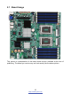
2.2 Block Diagram S8236 Block Diagram 11 http://www.tyan.
2.3 Board Parts, Jumpers and Connectors This diagram is representative of the latest board revision available at the time of publishing. The board you receive may not look exactly like the above diagram. But for the DIMM number please refer to the above placement for memory installation. For the latest board revision, please visit our web site at http://www.tyan.com. 12 http://www.tyan.
Jumpers & Connectors Jumper/Connector Function J4 COM2 Header J5/J12/J30/J34/J54/J55/J56 4-pin Fan Connectors J23 Front Panel Header J24 Reset Switch J25 Power Switch J28 Fan TACH Connector J29/J33 USB Front Panel Header J31 PSMI Connector J32 LAN3 Active LED Header J53 HDD Fault Header J59 IPMB Header JP1/JP2 COM2 Function Select Jumper JP3 Clear CMOS Jumper JP6 Front Panel ID LED Button JP7 Chassis Intrusion Header LED1 ID LED LED2 SAS Flash Ready (Amber) LED3 SAS HD F
LED Definitions LED2 LED3 SAS Flash Ready SAS HD Fault LED Pin + State OFF OFF Blinking Amber Pin + State OFF ON LED4 Power On LED LED5 Standby LED Pin + State OFF ON Pin + State OFF ON LED6 SAS Error LED Signal +3V SAS_FLASH_RY Description Pin + State OFF ON (SAS SKU Only) The SAS firmware is not updated. (SAS SKU Only) The LED shows blinking amber when the system is updating the SAS firmware.
LED7 LED8 SAS Heart Beat LED BMC Heart Beat LED Pin + State Signal +3V GND Description OFF OFF Blinking Green Pin + State Signal +3VSB GND Description OFF OFF Blinking Green The LED shuts off when the SAS controller can not be detected or properly initiated. The LED blinks per second to indicate that the SAS controller is working normally The LED shuts off when the BMC controller can not be detected or properly initiated.
J12 J56 J55 J30 J5 J34 J4 16 http://www.tyan.
J4: COM2 Connector Signal DCD RXD TXD DTR GND Pin 1 3 5 7 9 Pin 2 4 6 8 10 Signal DSR RTS CTS RI KEY J5/J12/J30/J34/J54/J55/J56: 4-Pin FAN Connectors Pin 1 2 3 4 Signal GND +12V TACH PWM Use this header to connect the cooling fan to your motherboard to keep the system stable and reliable.
J31 J29 LED1 J59 J33 J32 18 http://www.tyan.
J29/J33: USB Front Panel Connector Signal 5V Power DD+ GND KEY Pin 1 3 5 7 9 Pin 2 4 6 8 10 Signal 5V Power DD+ GND NC J31: PSMI Connector Pin Signal 1 2 PSMI_Clock 3 PSMI_Data PSU_Alert_L 4 5 GND 3.3V Standby LED1: ID LED Pin Signal + P3V3_AUX ID_SW_L State Color Description On Blue System identified Off Off System not identified NOTE: IPMI can activate ID LED from remote site. Please visit the TYAN Web Site at http://www.tyan.
JP6 JP1 JP2 JP7 20 http://www.tyan.
JP1/JP2: COM2 Function Switch Jumper 1 Pin 1-2 Closed: SIO to COM2 (Default) 3 1 Pin 2-3 Closed: BMC UART2 to COM2 3 JP3: Clear CMOS Jumper 1 3 Normal (Default) 1 3 Clear CMOS You can reset CMOS by using this jumper if you have forgotten your system/setup password or need to clear BIOS setting. 1. Power off system and disconnect both power connectors from the motherboard. 2. Use jumper cap to close Pin_2 and Pin_3 for seconds to Clear CMOS. 3.
2.4 Installing the Processor and Heat sink The S8236 supported AMD® processors are listed in section 1.2 Hardware Specifications on page 4. Check our website at http://www.tyan.com for latest processor support. NOTE: MiTAC is not liable for damage as a result of operating an unsupported configuration. Processor Installation (G34 1944-pin Socket for AMD CPU) Follow the steps below to install the processors and heat sinks.
3. Lift the socket cover to a fully open position. 4. Take off the CPU protection cap. 5. Place the CPU in the CPU socket and make sure that the gold arrow is located in the right direction with two notches properly aligned. 23 http://www.tyan.
6. Close the socket cover and press the CPU socket lever down to lock the CPU in place. 7. Repeat the same procedures to install the second CPU. Heat sink Installation After installing the processor, you should proceed to install the heat sink. The CPU heat sink will ensure that the processor do not overheat and continue to operate at maximum performance for as long as you own them. The overheated processor is dangerous to the motherboard.
2.5 Thermal Interface Material There are two types of thermal interface materials designed for use with the processors. The most common material comes as a small pad attached to the heat sink at the time of purchase. There should be a protective cover over the material. Take care not to touch this material. Simply remove the protective cover and place the heat sink on the processor. The second type of interface material is usually packaged separately. It is commonly referred to as ‘thermal compound’.
2.6 Tips on Installing Motherboard in Chassis Before installing your motherboard, make sure your chassis has the necessary motherboard support studs installed. These studs are usually metal and are gold in color. Usually, the chassis manufacturer will pre-install the support studs. If you are unsure of stud placement, simply lay the motherboard inside the chassis and align the screw holes of the motherboard to the studs inside the case.
Some chassis include plastic studs instead of metal. Although the plastic studs are usable, MiTAC recommends using metal studs with screws that will fasten the motherboard more securely in place. Below is a chart detailing what the most common motherboard studs look like and how they should be installed. 27 http://www.tyan.
2.7 Installing the Memory Before installing memory, ensure that the memory you have is compatible with the motherboard and processor. Check the TYAN Web site at http://www.tyan.com for details of the type of memory recommended for your motherboard. The following diagram shows common types of DDR3 memory modules.
Recommended Memory Population Table Single CPU Installed (CPU0 only) Quantity of memory installed 1 2 3 4 Dual CPU installed (CPU0 and CPU1) 6 CPU0_DIMM(1)D0 2 3 4 5 6 7 8 10 12 14 16 √ √ √ √ √ √ √ √ √ √ CPU0_DIMM(2)D1 √ √ CPU0_DIMM(3)C0 √ √ √ √ √ CPU0_DIMM(4)C1 √ √ CPU0_DIMM(5)B0 CPU0_DIMM(6)B1 √ √ √ CPU0_DIMM(7)A0 CPU0_DIMM(8)A1 8 √ √ √ √ √ √ √ √ √ √ √ √ √ √ √ √ √ √ √ √ √ √ √ √ √ √ √ √ √ √ √ √ √ √ √ √ √ √ √ √ √ √ √ √
http://www.tyan.
U-DIMM Module Support DDR3 Speed/Voltage 1.35v 1.5v 800MHz 800MHz 800MHz 800MHz 1066MHz 1066MHz 1066MHz 1066MHz 1066MHz 1333MHz 1066MHz 1333MHz DDR3 Rank Configuration DIMM1 DIMM0 (A1, B1, (A0, B0, C1, D1) C0, D0) SR and n/a DR SR and SR and DR DR SR and n/a DR SR and SR and DR DR SR and n/a DR SR and SR and DR DR Notes: U-DIMM can support up to 4GB sized DIMM’s Maximum of 8GB per channel SR and DR UDDR3 module support only x8 DRAM module support only SR and DR 1.
R-DIMM Module Support DDR3 Speed/Voltage DDR3 Rank Configuration 1.35v 1.
Memory Installation Procedure Follow these instructions to install memory modules into the S8236. 1. Press the locking levers in the direction shown in the following illustration. 2. Align the memory module with the socket. The memory module is keyed to fit only one way in the socket. KEY SLOT 3. Seat the module firmly into the socket by gently pressing down until it sits flush with the socket. The locking levers pop up into place. 33 http://www.tyan.
2.8 Attaching Drive Cables Attaching Serial ATA Cables S8236 is equipped with six Serial ATA (SATA) channel. Connections for the drives are very simple. There is no need to set Master/Slave jumpers on SATA drives. If you are in need of SATA/SAS cables or power adapters please contact your place of purchase. The following pictures illustrate how to connect an SATA drive. 1. SATA drive cable connection 2. SATA drive power connection 3. SATA cable motherboard connector 4.
2.9 Installing Add-In Cards Before installing add-in cards, it’s helpful to know if they are fully compatible with your motherboard. For this reason, we’ve provided the diagrams below, showing the slots that may appear on your motherboard. PCI-E Gen. 2 x16 slots (PCIE_1 & PCIE_2) NOTE: The PCIE_1 slot is designed to fit both add-on PCI-E card and riser card (M2091). However, The PCIE_2 slot is designed for riser card only (M2091-R).
2.10 Connecting External Devices Connecting external devices to the motherboard is an easy task. The motherboard supports a number of different interfaces through connecting peripherals. See the following diagrams for the details. RJ-45 LAN Port (LAN3) VGA Port LAN1 2 X USB Ports COM Port LAN2 2 x RJ-45 LAN Ports NOTE: Peripheral devices can be plugged straight into any of these ports but software may be required to complete the installation.
2.11 Installing the Power Supply There are three power connectors on your S8236. It is required that you have an EPS12V power supply which has one 24-pin and two 8-pin connectors. 24-pin (PW1) Signal Pin Pin Signal +3.3V 1 13 +3.3V +3.3V 2 14 -12V GND 3 15 GND +5V 4 16 PS_ON GND 5 17 GND +5V 6 18 GND +12V 7 19 GND Power OK 8 20 RES 5VSB 9 21 +5V +12V 10 22 +5V +12V 11 23 +5V +3.
2.12 Finishing Up Congratulations on making it this far! You have finished setting up the hardware aspect of your computer. Before closing up your chassis, make sure that all cables and wires are connected properly, especially IDE cables and most importantly, jumpers. You may have difficulty powering on your system if the motherboard jumpers are not set correctly. In the rare circumstance that you have experienced difficulty, you can find help by asking your vendor for assistance.
Chapter 3: BIOS Setup 3.1 About the BIOS The BIOS is the basic input/output system, the firmware on the motherboard that enables your hardware to interface with your software. The BIOS determines what a computer can do without accessing programs from a disk. The BIOS contains all the code required to control the keyboard, display screen, disk drives, serial communications, and a number of miscellaneous functions. This chapter describes the various BIOS settings that can be used to configure your system.
3.1.2 Getting Help Pressing [F1] will display a small help window that describes the appropriate keys to use and the possible selections for the highlighted item. To exit the Help Window, press [ESC] or the [F1] key again. 3.1.
3.2 Main Menu In this section, you can alter general features such as the date and time. Note that the options listed below are for options that can directly be changed within the Main Setup screen. Main Advanced BIOS Setup Utility PCI/PnP Boot Security Chipset Exit System Overview Use [ENTER], [TAB] or [SHIFT-TAB] to select a field AMIBIOS Version : vx.xx Build Date : DD/MM/YY ID : xxxx_xxx Use [+] or [-] to configure system time.
3.3 Advanced Menu This section facilitates configuring advanced BIOS options for your system. Main Advanced Advanced Settings BIOS Setup Utility PCI/PnP Boot Security Chipset Exit Configure CPU WARING: Setting wrong values in below sections may cause system to malfunction. CPU Configuration IDE Configuration Super IO Configuration ACPI Configuration Hardware Health Configuration IPMI 2.
3.3.1 Advanced CPU Configuration This section allows you to fine-tune the processor options. Main Advanced BIOS Setup Utility PCI/PnP Boot Security Configure advanced CPU settings Module Version: xx.xx Physical Count: xxxx Logical Count: xxxx Chipset Exit This should be enabled in order to enable or disable the “Enhanced Halt State”. Processor Information AMD Opteron (tm) Processor xxxx Revision: D1 Cache L1: xxKB Cache L2: xxxxKB Cache L3: xxxxKB Speed: xxxx , NB Clk: xxxx Able to change Freq.
ACPI SRAT Table Enable or disable the building of ACPI SRAT Table. Disabled / Enabled C1E Support Enable or disable the C1 Enhanced mode. Disabled / Enabled 44 http://www.tyan.
3.3.
3.3.2.1 SATA0 Sub-Menu Main Advanced BIOS Setup Utility PCI/PnP Boot Security SATA0 Exit Selects the type of device connected to the system. Device: Not Detected Type LBA /Large Mode Block (Multi-Sector Transfer) PIO Mode DMA Mode S.M.A.R.T. 32 Bit Data Transfer Chipset [Auto] [Auto] [Auto] [Auto] [Auto] [Auto] [Enabled] ← Select Screen ↑↓ Select Item Enter Go to Sub Screen F1 General Help F10 Save and Exit ESC Exit Type Selects the type of device connected to the system.
32-Bit Data Transfer Enable 32-bit to maximize the IDE hard disk data transfer rate. Enabled / Disabled 47 http://www.tyan.
3.3.3 Super I/O Configuration Main Advanced BIOS Setup Utility PCI/PnP Boot Security Configure Win627DHG Super IO Chipset Serial Port1 Address Serial Port2 Address [3F8/IRQ4] [2F8/IRQ3] Watchdog Mode Watchdog Timer [Disabled] [2] Chipset Exit Allows BIOS to Select Serial Port1 Base Addresses. ← Select Screen ↑↓ Select Item Enter Go to Sub Screen F1 General Help F10 Save and Exit ESC Exit Serial Port1 Address Allows BIOS to configure Serial Port1 Base Address.
3.3.4 ACPI Configuration Main Advanced BIOS Setup Utility PCI/PnP Boot Security ACPI Settings Chipset Exit Advanced ACPI Configuration settings ← Select Screen ↑↓ Select Item Enter Go to Sub Screen F1 General Help F10 Save and Exit ESC Exit Advanced ACPI Configuration 3.3.4.1 Advanced ACPI Configuration Main Advanced BIOS Setup Utility PCI/PnP Boot Security Advanced ACPI Configuration ACPI Version Features ACPI APIC support AMI OEMB table Headless mode [ACPI v3.
AMI OEMB Table Set this value to allow the ACPI BIOS to add a pointer to an OEMB table in the Root System Description Table (RSDT) table. Enabled / Disabled NOTE: OEMB table is used to pass POST data to the AMI code during ACPI O/S operations. Headless Mode Enable or disable Headless operation mode through ACPI. Disabled / Enabled 50 http://www.tyan.
3.3.
3.5.
3.3.6 IPMI 2.0 Configuration Main Advanced BIOS Setup Utility PCI/PnP Boot Security IPMI 2.0 Configuration Chipset Exit Status of BMC View BMC System Event Log Clear BMC System Event Log Set LAN Configuration Set VLAN Configuration Set PEF Configuration BMC Watch Dog Timer Action BMC Alert LED and Beep Working View all events in the BMC Event Log. It will take a max. of 15 seconds to read all BMC SEL records.
3.3.6.1 View BMC System Event Log Main Advanced Total Number of Entries: SEL Entry Number SEL Record ID SEL Record Type Event Timestamp Generator ID Event Message Format Ver Event Sensor Type Event Sensor Number Event Dir Type Event Data BIOS Setup Utility PCI/PnP Boot Security xxx Chipset Exit Use +/- to traverse the event log. [1] xxxx xxxx (System Event) MM DD, YYYY HH:MM:SS xxxx xx (IPMI Ver 2.
3.3.6.2.1 Setup LAN Configuration Main Advanced BIOS Setup Utility PCI/PnP Boot Security Setup LAN Configuration IP Address Configuration Chipset Exit IPMI IP Address Source STATIC/DHCP [DHCP] Save LAN Configuration ← Select Screen ↑↓ Select Item Enter Go to Sub Screen F1 General Help F10 Save and Exit ESC Exit IP Address Source Select IPMI IP Address Source. STATIC / DHCP NOTE: IP Address and Subnet Mask appear when IP Address Source is set to [STATIC].
3.3.6.3 Set VLAN Configuration Main Advanced BIOS Setup Utility PCI/PnP Boot Security Setup VLAN ID F Configuration Chipset Exit Press Enter and [OK] to save LAN configure [Enabled] [Enabled] [033] Current VLAN ID Status VLAN Tagging VLAN ID Save VLAN ID Configuration Current VLAN ID Status Read only. It can not be modified in user mode. VLAN Tagging Enable / Disable VLAN Tagging. Enabled / Disabled VLAN ID Enter VLAN ID. Save VLAN ID Configuration Press Enter and [OK] to save VLAN configure.
3.3.6.4 Set PEF Configuration Main Advanced BIOS Setup Utility PCI/PnP Boot Security Set PEF Configuration Parameters Command [Enabled] [Alert] [Disabled] [Disabled] [Disabled] PEF Support PEF Action Global Control Alert Startup Delay Startup Delay Event Message for PEF Action Chipset Exit Enable or Disable PEF Support ← Select Screen ↑↓ Select Item Enter Go to Sub Screen F1 General Help F10 Save and Exit ESC Exit PEF Support Enable or disable PEF support.
3.3.7 Remote Access Configuration Main Advanced BIOS Setup Utility PCI/PnP Boot Security Configure Remote Access type and parameters Remote Access [Disabled] Serial Port Number Base Address, IRQ Serial Port Mode Flow Control Redirection After BIOS POST Terminal Type VT-UTF8 Combo Key Support Sredir Memory Display Delay [COM1] [3F8h, 4] [38400 8, n, 1] [None] [Always] [ANSI] [Enabled] [No Delay] Chipset Exit Select remote access type.
VT-UTF8 Combo Key Support Enable VT-UFT8 Combination Key Support for ANSI/VT100 terminals. Enabled / Disabled Sredir Memory Display Delay Gives the delay in seconds to display memory information. No Delay / Delay 1 Sec / Delay 2 Sec / Delay 4 Sec 59 http://www.tyan.
3.3.8 USB Configuration Main Advanced BIOS Setup Utility PCI/PnP Boot Security USB Configuration Exit Enables support for legacy USB. AUTO option disables legacy support if no USB devices are connected. Module Version – x.xx.x – xx.x USB Devices Enabled: None Legacy USB Support USB 2.0 Controller Mode BIOS EHCI Hand-Off Legacy USB 1.
3.3.9 Onboard Devices Configuration Main Advanced BIOS Setup Utility PCI/PnP Boot Security Onboard Device and PCI Slots Configuration Onboard LAN 1/2 (82576) Onboard LAN 1 OP ROM Onboard LAN 2 OP ROM Onboard LAN 3 (82574) Onboard LAN 3 OP ROM [Enabled] [Disabled] [Disabled] [Enabled] [Disabled] Onboard SAS Onboard VGA [Enabled] [Enabled] Onboard Lan1/Lan2 (82576) Enable /disable Lan controller. Enabled / Disabled Onboard Lan1/Lan2 OP-ROM Execute Lan OP-ROM or not.
3.4 PCI/PnP Menu Main Advanced BIOS Setup Utility PCI/PnP Boot Security Chipset Exit Clear NVRAM during System Boot. Advanced PCI/PnP Settings WARING: Setting wrong values in below sections may cause system to malfunction.
PCI IDE Bus Master Enabled: BIOS uses PCI bus mastering for reading / writing to IDE drives. Enabled / Disabled 63 http://www.tyan.
3.5 Boot Menu Main Advanced BIOS Setup Utility PCI/PnP Boot Security Chipset Exit Configures settings during System Boot. Boot Settings Boot Settings Configuration Boot Device Priority Hard Disk Drives ← Select Screen ↑↓ Select Item Enter Go to Sub Screen F1 General Help F10 Save and Exit ESC Exit CD/DVD Drives 3.5.
Boot Up Num-Lock Selects Power-on state for Numlock. On / Off Wait for ‘F1’ If Error Waits for F1 key to be present if error occurs. Enabled / Disabled Hit ‘DEL’ Message Display Displays “Press DEL to run Setup in POST”. Enabled / Disabled Interrupt 19 Capture Enabled: allows option ROMs to trap interrupt 19. Enabled / Disabled Endless Boot Enable/Disable endless loop boot from BBS table. Enabled / Disabled 65 http://www.tyan.
3.5.2 Boot Device Priority Main Advanced BIOS Setup Utility PCI/PnP Boot Security Chipset Exit Specifies the boot sequence from the available devices. Boot Device Priority 1st Boot Device 2nd Boot Device [xx,xxx-xxxxx:xxx] [xx,xxx-xxxxx:xxx] A device enclosed in parenthesis has been disabled in the corresponding type menu. ← Select Screen ↑↓ Select Item Enter Go to Sub Screen F1 General Help F10 Save and Exit ESC Exit Set your boot device priority.
3.5.4 CD/DVD Drives Main Advanced BIOS Setup Utility PCI/PnP Boot Security Exit Specifies the boot sequence from the available devices. CD/DVD Drives 1st Boot Device Chipset [xx,xxx-xxxxx:xxx] A device enclosed in parenthesis has been disabled in the corresponding type menu. ← Select Screen ↑↓ Select Item Enter Go to Sub Screen F1 General Help F10 Save and Exit ESC Exit Specify the boot sequence from the available devices. 67 http://www.tyan.
3.6 Security Menu Main Advanced Security Settings BIOS Setup Utility PCI/PnP Boot Security Supervisor Password : Not Installed User Password : Not Installed Change Supervisor Password Change User Password Boot Sector Virus Protection [Disabled] Chipset Exit Install or change the password. ← Select Screen ↑↓ Select Item Enter Go to Sub Screen F1 General Help F10 Save and Exit ESC Exit Supervisor Password/User Password Read only. Change Supervisor Password Install or change the password.
3.7 Chipset Menu Main Advanced BIOS Setup Utility PCI/PnP Boot Security Chipset Exit Advanced Chipset Settings Configure CPU Bridge features. WARNING: Setting wrong values in below sections may cause system to malfunction. ← Select Screen ↑↓ Select Item Enter Go to Sub Screen F1 General Help F10 Save and Exit ESC Exit NorthBridge Configuration SouthBridge Configuration RD890 Configuration Allow you to change NorthBridge, SouthBridge and RD890 Configuration. 69 http://www.tyan.
3.7.
3.7.1.
3.7.1.2 ECC Configuration Main Advanced BIOS Setup Utility PCI/PnP Boot Security ECC Configuration ECC Mode DRAM ECC Enable DRAM SCRUB REDIRECT DRAM BG Scrub Data Cache BG Scrub L2/L3 Cache BG Scrub [Good] [Enabled] [Enabled] [1.31ms] [Disabled] [Disabled] Chipset Exit Set the level of ECC protection. Note: The “super” ECC mode dynamically sets the DRAM scrub rate so all of memory is scrubbed in 8 hours.
Disabled / 40ns / 80ns / 160ns / 320ns / 640ns / 1.28us / 2.56us / 5.12us / 10.2us/ 20.5us / 41.0us / 82.9us / 163.8us / 327.7us / 655.4us L2/L3 Cache BG Scrub Allow the L2/L3 Data Cache RAM to be corrected while idle. Disabled / 40ns / 80ns / 160ns / 320ns / 640ns / 1.28us / 2.56us / 5.12us / 10.2us/ 20.5us / 41.0us / 82.9us / 163.8us / 327.7us / 655.4us 73 http://www.tyan.
3.7.1.3 DRAM Timing Configuration Main Advanced BIOS Setup Utility PCI/PnP Boot Security DRAM Timing Configuration DRAM Timing Config [Auto] Chipset Exit Auto Manual ← Select Screen ↑↓ Select Item Enter Go to Sub Screen F1 General Help F10 Save and Exit ESC Exit DRAM Timing Config Select the DRAM Frequency programming method. If Auto, the DRAM speed will be based on SPDs. If Limit, the DRAM speed will not exceed the specified value. If Manual, the DRAM speed specified will be programmed by users.
3.7.2 South Bridge Configuration Main Advanced BIOS Setup Utility PCI/PnP Boot Security SouthBridge Chipset Configuration Chipset Exit Disabled Enabled SB700 CIMx Version: x.x.
Chassis Intrusion Detection Disabled: Disable Chassis Intrusion Detection. Enabled: When a chassis open event is detected, the BIOS will report the event. Disabled / Enabled SGPIO Function Enable or disable the SP5100 SGPIO function. Enabled / Disabled 76 http://www.tyan.
3.7.3 RD890 Configuration Main Advanced BIOS Setup Utility PCI/PnP Boot Security RD890 Configuration Chipset Exit Disabled Enabled PCI Express Configuration Hyper Transport Configuration IOMMU [Disabled] Primary Video Controller [PCIE GPP1-GPP2-PCI] ← Select Screen ↑↓ Select Item Enter Go to Sub Screen F1 General Help F10 Save and Exit ESC Exit IOMMU Disable or Enable IOMMU function.
3.7.3.
3.7.3.1.1 Port # 02/03/11/12 Features Main Advanced Gen2 High Speed Mode Link ASPM Slot Power Limit, W L1 Immediate ACK BIOS Setup Utility PCI/PnP Boot Security [Auto] [Disabled] [75] [Disabled] Chipset Exit Disabled: Force PCIE link speed to GEN1. ← Select Screen ↑↓ Select Item Enter Go to Sub Screen F1 General Help F10 Save and Exit ESC Exit Gen2 High Speed Mode Disabled: force PCIE link speed to GEN1. Auto / Disabled Link ASPM Active State Power Management.
3.7.3.1.2 Port # 04/09/13 Features Main Advanced BIOS Setup Utility PCI/PnP Boot Security Link ASPM L1 Immediate ACK [Disabled] [Disabled] Chipset Exit Active State Power Management ← Select Screen ↑↓ Select Item Enter Go to Sub Screen F1 General Help F10 Save and Exit ESC Exit Link ASPM Active State Power Management. Disabled / L0s / L1 / L0s & L1 / L0s Downstream / L0s Downstream + L1 L1 Immediate ACK When Enabled L1 will be ACK’d immediately. Disabled / Enabled 3.7.3.1.
3.7.3.1.3 GPP1/GPP2/GPP3a/GPP3b Core Setting Main Advanced Turn Off PLL During L1/L23 TXCLK Clock Gating in L1 LCLK Clock Gating in L1 BIOS Setup Utility PCI/PnP Boot Security [Enabled] [Enabled] [Enabled] Chipset Exit Enabled Disabled ← Select Screen ↑↓ Select Item Enter Go to Sub Screen F1 General Help F10 Save and Exit ESC Exit Turn Off PLL During L1/L23 Enabled / Disabled TXCLK Clock Gating in L1 Enabled / Disabled LCLK Clock Gating in L1 Enabled / Disabled 3.7.3.1.
3.7.3.2 Hyper Transport Configuration Main Advanced BIOS Setup Utility PCI/PnP Boot Security Hyper Transport Configuration HT Extended Address HT3 Link Power State HT Link Tristate [Disabled] [Auto] [Auto] HT Extended Address Enabled: HT supports 52-bit physical addressing. Disabled: HT supports 40-bit physical addressing. Disabled / Enabled / Auto HT3 Link Power State Select the HT3 Link Power State. Auto / LS0 / LS1 / LS2 / LS3 HT Link Tristate Select the HT1 Link Tristate mode.
3.8 Exit Menu Main Advanced BIOS Setup Utility PCI/PnP Boot Security Chipset Exit Exit Options Exit system setup after saving the changes. Save Changes and Exit Discard Changes and Exit Discard Charges F10 key can be used for this operation. ← Select Screen ↑↓ Select Item Enter Go to Sub Screen F1 General Help F10 Save and Exit ESC Exit Load Optimal Defaults Load Failsafe Defaults Save Changes and Exit Use this option to exit setup utility and re-boot.
NOTE 84 http://www.tyan.
Chapter 4: Diagnostics NOTE: if you experience problems with setting up your system, always check the following things in the following order: Memory, Video, CPU By checking these items, you will most likely find out what the problem might have been when setting up your system. For more information on troubleshooting, check the TYAN website at http://www.tyan.com. 4.1 Beep Codes Fatal errors, which halt the boot process, are communicated through two kinds of audible beeps.
4.3 AMIBIOS Post Code The POST code checkpoints are the largest set of checkpoints during the BIOS preboot process. The following table describes the type of checkpoints that may occur during the POST portion of the BIOS: Checkpoint 03 04 05 06 08 0A 0B 0C 0E 13 24 30 2A 2C 2E 31 33 37 Description Disable NMI, Parity, video for EGA, and DMA controllers. Initialize BIOS, POST, Runtime data area. Also initialize BIOS modules on POST entry and GPNV area.
Checkpoint 38 39 3A 3B 3C 40 50 52 60 75 78 7A 7C 84 85 87 8C 8E 90 A0 A1 A2 A4 A7 A8 A9 AA AB AC B1 00 Description Initializes different devices through DIM. See DIM Code Checkpoints section of document for more information. Initializes DMAC-1 & DMAC-2. Initialize RTC date/time. Test for total memory installed in the system. Also, Check for DEL or ESC keys to limit memory test. Display total memory in the system. Mid POST initialization of chipset registers.
NOTE 88 http://www.tyan.
Glossary ACPI (Advanced Configuration and Power Interface): a power management specification that allows the operating system to control the amount of power distributed to the computer’s devices. Devices not in use can be turned off, reducing unnecessary power expenditure. AGP (Accelerated Graphics Port): a PCI-based interface which was designed specifically for demands of 3D graphics applications. The 32-bit AGP channel directly links the graphics controller to the main memory.
Bus: a data pathway. The term is used especially to refer to the connection between the processor and system memory, and between the processor and PCI or ISA local buses. Bus mastering: allows peripheral devices and IDEs to access the system memory without going through the CPU (similar to DMA channels). Cache: a temporary storage area for data that will be needed often by an application. Using a cache lowers data access times since the information is stored in SRAM instead of slower DRAM.
DRAM (Dynamic RAM): widely available, very affordable form of RAM which looses data if it is not recharged regularly (every few milliseconds). This refresh requirement makes DRAM three to ten times slower than non-recharged RAM such as SRAM. ECC (Error Correction Code or Error Checking and Correcting): allows data to be checked for errors during run-time. Errors can subsequently be corrected at the same time that they’re found.
I/O (Input/Output): the connection between your computer and another piece of hardware (mouse, keyboard, etc.) IRQ (Interrupt Request): an electronic request that runs from a hardware device to the CPU. The interrupt controller assigns priorities to incoming requests and delivers them to the CPU. It is important that there is only one device hooked up to each IRQ line; doubling up devices on IRQ lines can lock up your system. Plug-nPlay operating systems can take care of these details for you.
RAID (Redundant Array of Independent Disks): a way for the same data to be stored in different places on many hard drives. By using this method, the data is stored redundantly and multiple hard drives will appear as a single drive to the operating system. RAID level 0 is known as striping, where data is striped (or overlapped) across multiple hard drives, but offers no fault-tolerance. RAID level 1 is known as mirroring, which stores the data within at least two hard drives, but does not stripe.
Standby mode: in this mode, the video and hard drives shut down; all other devices continue to operate normally. UltraDMA-33/66/100: a fast version of the old DMA channel. UltraDMA is also called UltraATA. Without a proper UltraDMA controller, your system cannot take advantage of higher data transfer rates of the new UltraDMA/UltraATA hard drives. USB (Universal Serial Bus): a versatile port. This one port type can function as a serial, parallel, mouse, keyboard or joystick port.
Technical Support If a problem arises with your system, you should first turn to your dealer for direct support. Your system has most likely been configured or designed by them and they should have the best idea of what hardware and software your system contains. Hence, they should be of the most assistance for you.
NOTE: A receipt or copy of your invoice marked with the date of purchase is required before any warranty service can be rendered. You may obtain service by calling the manufacturer for a Return Merchandise Authorization (RMA) number. The RMA number Should be prominently displayed on the outside of the shipping carton and the package should be mailed prepaid. ® TYAN will pay to have the board shipped back to you.