Tyan S1854 Trinity 400 Motherboard Users Manual Revision 2.00 Copyright © Tyan Computer Corporation, 2000. All rights reserved. No part of this manual may be reproduced or translated without prior written consent from Tyan Computer Corp. All registered and unregistered trademarks and company names contained in this manual are property of their respective companies including, but not limited to the following. Award is a trademark of Phoenix Technologies Ltd.
Table of Contents 1. Introduction.................................................................................................. 4 Overview.............................................................................................4 Icons................................................................................................. 5 Chipset Hardware Specifications/Feaures.................................... 6 Technical Support...........................................................................
4. System Resources......................................................................................63 Beep Codes..................................................................................... 63 Troubleshooting System Problems..............................................64 Displayed Error Messages.............................................................64 Appendix -1 Glossary.....................................................................................
Chapter 1 chapter 1 Introduction Introduction Overview The S1854 Trinity 400 is a quality, high performance motherboard designed for Socket 370 Intel Celeron and Slot 1 Intel PII/ PIII microprocessors. The Trinity 400 utilizes the VIA VT82C694X with Award BIOS for S1854 & S1854-A models. S1854 can support Celeron/ PII/ PIII CPU speeds of 300MHz through 750MHz, and host bus speeds of 66MHz to 133MHz, the VIA chipsets bus speed is Auto-Determined by the CPU.
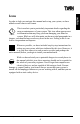
In order to help you navigate this manual and set up your system, we have added several icons to our format. This icon alerts you to particularly important details regarding the setup or maintenance of your system. This icon often appears next to information that may keep you from damaging your board or important! system. While we will often point out the most vital paragraphs in a chapter, you should always read every word in the text. Failing to do so can lead to exasperation and expense.
Chapter 1 Introduction Hardware Specifications/Features Processor Information One Socket 370 CPU connector One Slot 1 CPU connector 66/ 100 / 133MHz bus support (auto-deter mined by CPU) Celeron 300 to 533MHz Pentium II and Pentium III up to 750MHz Chipset Information VIA Apollo Pro 133:VT82C694X+VT82C596B Winbond 977 EF Super I/O chipset Voltage and Power Information ATX power supply connector +12V power source for DC fan onboard 3.3V DRAM support Main Memory Up to 768MB onboard (1.
Two PCI bus mastering EIDE channels Supports EIDE CD-ROMs PIO Mode 3 & 4 (up to 17MB/sec DTR) UltraDMA/66 bus mastering mode (up to 66MB/sec DTR) Support for two floppy drives (up to 1.44MB) Two serial ports (16550 UARTs) One ECP/EPP parallel port One IR (InfraRed) I/O interface port header Two USB rev 1.
Chapter 1 Introduction Technical Support If a problem arises with your system, you should turn to your dealer for help first. Your system has most likely been configured by them, and they should have the best idea of what hardware and software your system contains. Hence, they should be of the most assistance.
This page left blank intentionally.
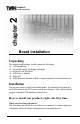
Chapter 2 chapter 2 Board Installation Board Installation Unpacking The motherboard package should contain the following: (1) S1854 mainboard (1) 40-pin IDE and 34-pin floppy cable pack (1) 80-pin ATA-66 IDE cable (1) S1854 Users Manual (1) Driver CD (1) URM Retention Module (URM is shipped mounted on the motherboard) Installation You are now ready to install your motherboard. The mounting hole pattern of the S1854 matches the ATX system board specifications.
Here are some precautions you should follow when installing your motherboard: Having reviewed the precautions above, the next step is to take the motherboard out of the cardboard box and static bag, hold it by its edges, and place it on a grounded antistatic surface, component side up. Inspect the board for damage.
Chapter 2 Board Installation Quick References for Jumpers In this manual, the terms closed and on are used when referring to jumpers (or jumper pins) that are active; open and off are used when referring to jumpers (or jumper pins) that are inactive. See the Figure 2-1 for examples of on and off pins and jumpers. Jumpers and pins are connected by slipping the plastic jumper connector overtop of two adjacent jumper pins (indicated by 1-2 or 2-3).
J22 (Video) J21 1 Creative ES1373 CON3 (WOL) 1 1 CON2 (WOR) DIMM bank 3 DIMM bank 2 1 Secondary IDE connector FAN4 1 1 J23 (CD) 1 AGP port 1 PCI slot 1 J16 J7 PCI slot 2 PCI slot 3 JP10 JP11 JP12 JP13 Joystick 1 VIA VT82C694X DIMM bank 1 Printer Port Slot 1 Type CPU COM1 Socket 370 CPU 1 Floppy drive connector USB0 Primary IDE connector PGA370 COM2 (Onboard Audio Optional) Microphone in Line in Line out ATX power connector FAN1 1 Mouse VIA VT82C596B PCI slot 4 1 D31 FAN3
Chapter 2 Board Installation Figure 2-4 : Map of S1854 Features PS/2 Mouse & Keyboard ports 4x AGP port 2-ch EIDE 6 PCI slots Via Apollo Pro Plus 133A AGPset BIOS Joystick / Audio ports (Onboard Audio Optional) 3 DIMM slots Floppy port 1 Parallel, 2 Com ports 2 USB ports Slot 1 Type for Pentium II/III CPU ATX power supply header Fuse 1, 2 Socket 370 for Celeron CPU Battery 1 ISA slot http://www.tyan.
! Important! important! Pleae note: In some versions of the S1854 board, there is an extra jumper setting (JP21) for CPU SELECTION. If you are using a Slot 1 Type CPU, please close the jumper, if your CPU is a socket please leave the jumper open. JP21(CPU Select) Warning: If JP21 is set to the incorrect CPU type, there will be no video display at Post. Please correct the jumper setting and reboot the system.
Chapter 2 Board Installation ! important! 1. Setting Jumpers 1-A. CPU Speed Settings (Jumpers JP10, JP11, JP12, JP13) There are two steps to set the CPU speed. First, set the clock multiplier with jumpers JP10 -13 according to the specification of your CPU using the chart below. After the system is ready to boot the BUS Speed is auto-detected. Presently all Celeron CPUs use a 66MHz bus speed. (Tyan does not recommend operating CPUs, memory, or PCI Bus at higher than rated speed.
8 Ground VCC 9 10 NC. IRRX 11 12 Power +5V Ground 13 14 N.C IRTX 15 16 N.C RESV 17 18 N.C 3 4 LED Yellow Power LED: For 2-pin: bicolor/single color - Use pins 2-4 For 3-pin: Use jumper D31. Buz Buz LED - Pwr/Slp LEDs 6 Power On/Off 7 2 LED Green Power (Sleep) Switch HDD LED 5 Reset Infrared Ground 1 J16 2 4 6 8 10 12 14 16 18 1 3 5 7 9 11 13 15 17 To p Bottom 1-C. Speaker Connector (Jumper J12) The speaker should be connected to pins 1-4 of jumper J12.
Chapter 2 Board Installation 1-G Soft Power Connector The Soft Power Connector is part of jumper block J16. The Trinity 400 uses the chipset for power management, including turning on and off the system. If the Power Button Function option in the BIOS Power Management Menu is set to On/Off (which is the default), pressing the power button once after the BIOS has booted up will turn the system on and off.
1-K Power LED Connector Jumper D31 is a three pin power LED header that can be used if you have a 3 pin Power LED. Otherwise refer to panel connector J16 for 2 pin LEDs. 3 pin LEDs can still be used on J16 where pin 13 would be for the Ground pin. CMOS RTC Flash EEPROM The Trinity 400 uses flash memory to store BIOS firmware. It can be updated as new versions of the BIOS become available. You can upgrade your BIOS easily using the flash utility (see page 60). 2.
Chapter 2 Board Installation 3. Installing Memory Since TYAN boards are manufactured with performance in mind, you should use add-in components that match. It is highly recommended that the memory DIMMs are installed prior to connecting the power supply. Some DIMM modules may seem to be high quality because of name or feel but that does not guarantee real-world usability.
INSTALL Figure 2-5* *Note: The image above is used to illustrate a concept and may not represent the actual image of your motherboard. To install your DIMMs, line your module up so that the pins fit into the slot. There is only one way that your DIMM can fit properly. Make sure that the short row of pins is lined up with the short gap in the DIMM slot. Figure 2-5 shows how to sit the DIMM into its slot. To insert the DIMM, push down vertically on the module with even force, as shown in the photo.
Chapter 2 Board Installation Figure 2-6* *Note: The image above is used to illustrate a concept and may not represent the actual image of your motherboard. The Trinity 400 uses a 64-bit data path from memory to CPU and can accommodate up to 768MB of SDRAM. The 168-pin DIMMs (Dual In-line Memory Modules) must be of the 3.3V, unbuffered variety. The position of the notch in the SDRAM key position will tell you whether or not a DIMM is unbuffered (see the Figure 2-7 below).
Some details of memory installation: At least one unbuffered DIMM must be installed for the system to POST. The mainboard supports 32MB, 64MB, 128MB and 256MB SDRAM.
Chapter 2 Board Installation 4. Installing the CPU and Cooling Fan Socket 370 type Celeron processors (300 through 533MHz) and Slot 1 type Pentium II/III can be used on the Trinity 400. Please refer to page 15 for the correct CPU jumper settings for your CPU. Remember: The CPU is a sensitive electronic component and it can easily be damaged by static electricity. Do not touch the CPU pins with your fingers. You should be able to insert the CPU into the socket with virtually zero force.
Installing Slot1 Type CPUs Figure 2-9b Figure 2-9a *Installing CPU Retention Modules* Note: Tyan provides a variety of retention modules. For detailed installation procedures of your module, please refer to Appendix 2 located at the back of the manual. Figure 2-10 below shows a side view of a retention brace securing both sides of the SECC2 CPU. When both sides are properly positioned, press both braces against the sides of the CPU and carefully lift them over the CPU slot on the motherboard.
Chapter 2 Board Installation Figure 2-11 Line up the retention brace with the holes provided on the motherboard. At the same time, make sure the CPU is lined up with the CPU slot. Lower the CPU onto the motherboard. The mountings on the retention brace should fit through the holes of the motherboard and the CPU should fit into the slot. (See Figure 2-11). Secure the retention brace. The end result should look like Figure 2-12.
INSTALL Figure 2-13 Removing CPU When removing the CPU, pull lightly on the pegs sucuring the retention brace and remove the CPU and retention brace at once. This may require careful firm tugs to pull the CPU out of its slot. 5. Connecting IDE and Floppy Drives The colored stripe on a ribbon cable should face toward the battery on the motherboard. Make sure that Pin 1 (denoted by a red stripe) is connected so that it is next to the power connector of the drive.
Chapter 2 Board Installation Pin 1 Figure 2-14 *Note: The image above is used to illustrate a concept and may not represent the actual image of your motherboard. Some symptoms of incorrectly installed HDDs are: Hard disk drives are not auto-detected: may be a Master/Slave problem or a bad IDE cable. Contact your vendor. Hard Disk Drive Fail message at bootup: may be a bad cable or lack of power going to the drive. No video or beeps onbootup: usually means the cable is on back wards.
Some symptoms of incorrectly installed floppies are: Floppy drives are not detected: usually caused by faulty cables, backward cables, or a bad floppy or motherboard. Try another single floppy drive to verify the problem or try another cable. Also, check to see if the onboard floppy is enabled in the BIOS. Floppy Drive Fail message at bootup: the cable, floppy, or motherboard may be faulty. Try another cable or floppy drive to verify.
Chapter 2 Board Installation warning NEVER plug an ISA card into a PCI slot or a PCI card in an ISA slot. You will void your warranty and damage your system board if you do this. When plugging the card in, especially when installing long cards, try to push the entire card in at one time. Dont force one end of the card into the socket first and then the other. This will create a rocking motion between the card and the slot and it will damage the pins within the socket.
Mouse Figure 2-16 Figure 2-17 Connecting Com and Printer Ports Figure 2-18 warning Warning: When plugging in your keyboard and mouse, or when plugging anything into a serial or Com port, make sure that the power is off. Connecting these devices and ports while the power is on is called hot plugging, and may damage your system.Figure 2-18 above shows the ATX double row connectors on this board. The Com and Printer ports, as well as the other ports, are labeled.
Chapter 2 Board Installation 8. Connecting the Power Supply Tyan recommends using an ATX power supply that conforms to industry standard revision 2.01. The Trinity 400 motherboard comes equipped with one onboard power connector. Figure 2-16 below shows an ATX power connector. When plugging in the power connector, make sure that the plastic clip on the power connector is aligned with the plastic tab on the onboard connector (see Figure 2-17 below).
chapter 3 INSTALL BIOS Configuration Introduction to Setup ! important! The BIOS section of the manual is subjected to change without notice and is provided here for reference purposes only. The settings and configurations of the BIOS are current at the time of print, although they may not be exactly the same as that displayed on your screen. This manual describes the Award BIOS Setup program. The Setup program lets you modify basic system configuration settings.
Chapter 3 BIOS Configuration Starting Setup The Award BIOS is immediately activated when you first turn on the computer. The BIOS reads system configuration information in CMOS RAM and begins the process of checking out the system and configuring it through the poweron self test (POST). When these preliminaries are finished, the BIOS seeks an operating system on one of the data storage devices (hard drive, floppy drive, etc.).
Ke y Up arrow Function Move to previous item. Down arrow Move to next item. Left arrow Move to iten on the left hand. Right arrow Move to item on the right hand. Esc key PgUp key Main Menu: Q uit and do not save changes into CMO S RAM. Status Page Setup Menu: Exit current page and return to Main Menu. Increase the numeric value or make changes. Decrease the numeric value or make changes. + key Increase the numeric value or make changes. - key Decrease the numeric value or make changes.
Chapter 3 BIOS Configuration Setup Variations Not all systems have the same Setup. While the basic look and function of the Setup program remains the same for all systems, the appearance of your Setup screens may differ from the screens shown here. Each system design and chipset combination require custom configurations. In addition, the final appearance of the Setup program depends on your system designer.
Standard CMOS Setup Options in the original PC AT-compatible BIOS. BIOS Features Setup Award Software enhanced BIOS options. Chipset Features Setup Options specific to your system chipset. Power Management Setup Advanced Power Management (APM) options. Integrated Peripherals I/O subsystems that depend on the integrated peripherals controller in your system. Supervisor/User Password Change, set, or disable a password.
Chapter 3 BIOS Configuration Standard CMOS Setup In the Standard CMOS menu you can set the system clock and calendar, record disk drive parameters and the video subsystem type, and select the type of errors that stop the BIOS POST. ROM PCI/ISA BIOS (TYAN1854) STANDARD CMOS SETUP AWARD SOFTWARE, INC.
HARD DISKS The BIOS supports up to four IDE drives. This section does not show information about other IDE devices, such as a CD-ROM drive, or about other hard drive types, such as SCSI drives. Note: We recommend that you select type auto for all drives. Here is a brief explanation of drive specifications: Type: The BIOS contains a table of pre-defined drive types.
Chapter 3 BIOS Configuration Drive A Select the correct specifications for the diskette drive(s) installed in the computer. None No diskette drive installed 360K , 5.25 in 5- 1/4 inch PC- type standard drive; 360 kilobyte capacity 1.2M, 5.25 in 5- 1/4 inch AT- type high- density drive; 1.2 megabyte capacity 720K , 3.5 in 3- 1/2 inch double- sided drive; 720 kilobyte capacity 1.44M, 3.5 in 3- 1/2 inch double- sided drive; 1.44 megabyte capacity 2.88M, 3.5 in 3- 1/2 inch double- sided drive; 2.
Memory You cannot change any values in the Memory fields; they are only for your information. The fields show the total installed random access memory (RAM) and amounts allocated to base memory, extended memory, and other (high) memory. RAM is counted in kilobytes (KB: approximately one thousand bytes) and megabytes (MB: approximately one million bytes). RAM is the computers working memory, where the computer stores programs and data currently being used, so they are accessible to the CPU.
Chapter 3 BIOS Configuration ROM PCI/ISA BIOS (TYAN1854) BIOS FEATURES SETUP AWARD SOFTWARE, INC.
Settings Chart (Continued) Setting Option D000-D3FFF Shadow D4000-D7FFF Shadow D8000-DBFFF Shadow DC000-DFFFF Shadow BIOS Default Disabled Disabled Disabled Disabled Setup Default Disabled Disabled Disabled Disabled Virus Warning When enabled, you receive a warning message if a program (specifically, a virus) attempts to write to the boot sector or the partition table of the hard disk drive. You should then run an anti-virus program.
Chapter 3 BIOS Configuration Swap Floppy Drive This option allows you to swap the floppy drives if more than one is installed. It allows you to switch the A: and B: to make B: become A: . Boot Up NumLock Status Toggle between On or Off to control the state of the NumLock key when the system boots. When toggled On, the numeric keypad generates numbers instead of controlling cursor operations. IDE HDD Block Mode Enables multi-sector transfers from the IDE drive in PIO mode.
Security Option If you have set a password, select whether the password is required every time the System boots, or only when you enter Setup. PCI/VGA Palette Snoop Your BIOS Setup many not contain this field. If the field is present, leave at Disabled. OS Select for DRAM > 64MB Select OS2 only if you are running OS/2 operating system with greater than 64 MB of RAM on your system. Video BIOS Shadow Software that resides in a read-only memory (ROM) chip on a device is called firmware.
Chapter 3 BIOS Configuration Chipset Features Setup This section describes features of the VIA Appollo Pro Plus 133A chipset. Advanced Options The parameters in this screen are for system designers, service personnel, and technically competent users only. Do not reset these values unless you understand the consequences of your changes. Note: This chapter describes all fields offered by Award Software in this screen. Your system board designer may omit or modify some fields.
Chipset Features Setup - Default Settings Chart BIOS Def ault Setup Def ault Bank 0/1 DRAM Timing SDRAM 10ns SDRAM 10ns Bank 2/3 DRAM Timing SDRAM 10ns SDRAM 10ns Bank 4/5 DRAM Timing SDRAM 10ns SDRAM 10ns SDRAM Cycle Length 3 3 DRAM Clock Host CLK 33M Host CLK-33M Memory Hole Disabled Disabled P2C/C2P Concurrency Enabled Enabled Fast R-W Turn Around Disabled Enabled CPU IOQ Size 1 Level 1 Level System BIOS Cacheable Disabled Enabled Video RAM Cacheable Disabled Enabled AG
Chapter 3 BIOS Configuration Video RAM Cacheable Increases video performance by caching video memory. AGP Aperture Size Select the size of the Accelerated Graphics Port (AGP) aperture. The aperture is a portion of the PCI memory address range dedicated for graphics memory address space. Host cycles that hit the aperture range are forwarded to the AGP without any translation. See www.agpforum.org for AGP information.
Power Management Setup Note: This chapter describes all fields offered by Award Software in this screen. Your system board designer may omit or modify some fields. ROM PCI/ISA BIOS (TYAN1854) POWER MANAGEMENT SETUP AWARD SOFTWARE, INC. : Enabled : User Define : No : Suspend->Off : V/H SYNC+Blank : 3 : Delay 4 sec.
Chapter 3 BIOS Configuration Setting Option VGA LPT & COM HDD & FDD DMA/master Modem Ring Resume RTC Alarm Resume Wake Up on LAN Primary INTR IRQ3 (COM2) IRQ4 (COM1) IRQ5 (Free) IRQ6 (Floppy Disk) IRQ7 (LPT1) IRQ8 (RTC Alarm) IRQ9 (Free) IRQ10 (Free) IRQ11 (Free) IRQ12 (PS/2 Mouse) IRQ13 (Coprocessor) IRQ14 (Primary IDE) IRQ15 (Secondary IDE) BIOS Default OFF LPT / COM ON OFF Disabled Disabled Disabled ON Primary Primary Primary Primary Primary Disabled Secondary Secondary Secondary Primary Disabled Prima
Video Off Option Selects the power-saving modes during which the monitor goes blank. Always O n Monitor remains on during power- saving modes. Suspend - - > O ff Monitor blanked when system enters Suspend mode. All Modes- - > O ff Monitor blanked when system enters any power- saving mode. Video Off Method Determines the manner in which the monitor is blanked. The Blank Screen option will let the system BIOS blank the screen when disabling video.
Chapter 3 BIOS Configuration Doze Mode After the selected period of system inactivity (1 minute to 1 hour), the CPU clock runs at slower speed while all other devices still operate at full speed. Suspend Mode After the selected period of system inactivity (1 minute to 1 hour), all devices except the CPU shut off. ** PM Events ** A power management (PM) event awakens the system from, or resets activity timers for, Suspend mode.
system by sending an interrupt request. When the system is in Suspend mode, IRQ activity can cause a Primary or Secondary wake-up. When Primary INTR is On, the IRQs in the above fields can be configured as Primary, Secondary, or Disabled. Primary Secondary The system wakes up fully when it detects IRQ activity. The system does not wake up, but the interrupt request is processed.
Chapter 3 BIOS Configuration PnP/PCI Configuration Note: This chapter describes all fields offered by Award Software in this screen. Your system board designer may omit or modify some fields. ROM PCI/ISA BIOS (TYAN1854) PNP/PCI CONFIGURATION AWARD SOFTWARE, INC.
PNP OS Installed Select Yes if the system operating environment is Plug-and-Play aware (e.g., Windows 98, Windows 2000). Resources Controlled By The Plug and Play EliteBIOS can automatically configure all the boot and Plug and Play-compatible devices. If you select Auto, all the interrupt request (IRQ) and DMA assignment fields disappear, because the BIOS automatically assigns them.
Chapter 3 BIOS Configuration AGP Master 1 WS Read Select Enabled to add one clock tick to AGP read operations. Assign IRQ for VGA Assign an IRQ number to your VGA adapter. http://www.tyan.
Integrated Peripherals Note: This chapter describes all fields offered by Award Software in this screen. Your system board designer may omit or modify some fields. ROM PCI/ISA BIOS (TYAN1854) INTEGRATED PERIPHERALS AWARD SOFTWARE, INC.
Chapter 3 BIOS Configuration Settings Chart (Continued) Setting Options BIOS Default Onboard Serial Port 1 3F8 / IRQ4 Setup Default 3F8 / IRQ4 Onboard Serial Port 2 2F8 / IRQ3 2F8 / IRQ3 UART Mode Normal Normal Onboard Parallel Port 378 / IRQ7 378 / IRQ7 Onboard Parallel Mode SPP SPP PWRON After PWR-Fail Off Off On-Chip PCI IDE First/Second Channel This chipset contains a PCI IDE interface with support for two IDE channels.
POWER ON Function This option enables power on from Windows 98 keyboard, right or left mouse button, password, hotkey, or power button. Note: If you use the keyboard password option to power on your system, the power button will be disabled. KBC Input Clock Allows you to adjust the keyboard clock signal. Onboard FDC Controller Select Enabled if your system has a floppy disk controller (FDC) installed on the system board and you wish to use it.
Chapter 3 BIOS Configuration User Password When you select this function, a message appears at the center of the screen: ENTER PASSWORD: Type the password, up to eight characters, and press Enter. Typing a password clears any previously entered password from CMOS memory. Now the message changes: CONFIRM PASSWORD: Again, type the password and press Enter. To abort the process at any time, press Esc.
Note: You should always clear your CMOS after flashing a BIOS. This will clear out any stray settings from your old BIOS which may have been carried over from the flashing process. Most problems encountered after flashing a BIOS will be solved by this simple procedure (see Hardware CMOS & Password Reset, page 16). To reprogram the system BIOS, the CPU must be running in real mode. FMW will not run if the CPU is operating in a protected or virtual mode.
Chapter 3 BIOS Configuration FLASH MEMORY WRITER V.7.3 AWARD SOFTWARE 1999 All Rights Reserved Flash TypeFile Name to Program: Error Message: Type in the whole file name, e.g. 1854v100.BIN, and confirm that you want to program the BIOS. The utility will then Blank, Erase, and Program the flash memory on the mainboard with the new BIOS file. You should choose Yes to save the original system BIOS to a floppy diskette before you program the new BIOS.
chapter 4 System Resources Fatal errors, which halt the boot process, are communicated through a series of audible beeps. If Award BIOS POST can initialize the system video display, it displays the error message. Displayed error messages, in most cases, allow the system to continue to boot. Displayed error messages are described on pages 64-65. See the top of the next page for the beep code chart.
Chapter 4 System Resources Troubleshooting System Problems Currently the only beep code indicated that a video error has occured and the BIOS cannot initialize the video screen to display any additional information. This beep code consists of a single long beep followed by two short beeps.
Error M e s s age Explanation 8042 Gate- A20 Error Gate A20 on the keyboard controller (8042) is not working. Replace the 8042. Address Line Short! Error in the address decoding circuitry. C: Drive Error No response from drive C:. Run the AMIDiag Hard Disk Utility. Check the C: hard disk type in Standard Setup. C: Drive Failure No response from hard disk drive C:. Replace the drive. Cache Memory Bad, Do Not Enable Cache! Cache memory is defective. Run AMIDiag. An AT system has two timers.
Chapter 4 System Resources Error M e s s age D: drive failure Diskette Boot Failure Display Switch Not Proper DMA Error Explanation No response from hard disk drive D:. Replace the drive. The boot diskette in drive A: cannot be used to boot the system. Use another boot diskette and follow the screen instructions. Some systems require a video switch be set to either color or monochrome. Turn the system off, set the switch properly, then power on. Error in the DMA controller.
Appendix 1 Glossary ACPI (Advanced Configuration and Power Interface) is a power management specification that allows the operating system to control the amount of power distributed to the computers devices. Devices not in use can be turned off, reducing unnecessary power expenditure. AT was the original form factor of IBMs PC. ATAPI (AT Attachment Packet Interface), also known as IDE or ATA, is a drive implementation that includes the disk controller on the device itself.
Appendix Glossary data the bus, phone line, or other electrical path, can carry. Greater bandwidth, then, also results in greater speed. The BIOS (Basic Input/Output System) program resides in the ROM chip, and provides the basic instructions for controlling your computers hardware. Both the operating system and application software use BIOS routines to ensure compatibility.
The COM port is another name for the serial port, which is so-called because it transmits the eight bits of a byte of data along one wire, and receives data on another single wire (that is, the data is transmitted in serial form, one bit after another). Parallel ports transmit the bits of a byte on eight different wires at the same time (that is, in parallel form, eight bits at the same time).
Appendix Glossary Firmware is low level software that controls the system hardware. Form factor is an industry term for the size, shape, power supply type, and external connector type of the PCB (personal computer board) or motherboard. The standard form factors are the AT and ATX, although TYAN also makes some Baby-AT boards. A Global timer is an onboard hardware timer, such as the Real Time Clock. Handshaking is a form of encryption.
NVRAM ROM and EEPROM are both examples of Non-Volatile RAM, memory that holds its data without power. DRAM, in contrast, is volatile. OEMs (Original Equipment Manufacturers) like Compaq or IBM package other companies motherboards and hardware inside their case and sell them. The parallel port transmits the bits of a byte on eight different wires at the same time (that is, in parallel form, eight bits at the same time). PCI stands for Peripheral Component Interconnect.
Appendix Glossary reconfigure your system each time you add or change any part of your hardware. The term RAM (Random Access Memory), while technically referring to a type of memory where any byte can be accessed without touching the adjacent data, is often used to refer to the systems main memory. This memory is available to any program running on the computer.
Universal Serial Bus or USB, is a versatile port. This one port type can function as a serial, parallel, mouse, keyboard, or joystick port. It is fast enough to support video transfer, and is capable of supporting up to 127 daisy-chained peripheral devices. VGA (Video Graphics Array) is the PC video display standard. V-SYNC controls the vertical properties of the monitor. ZIF socket Zero Insertion Force sockets make it possible to insert CPUs without damaging the sensitive pins.
Appendix 2 Appendix 2 Retention Module installation Retention Module Installation Installing SECC2 CPUs -Option 1 The following are alternative methods of installing the CPU and retention module to that of chapter 2. On both sides of the SECC2 CPU reside the lower tabs of the aluminum heat sink (see Figure A below). These tabs should snap into the retention module. Currently, the retention module recommended for securing the SECC2 CPU is included in the motherboard package.
Line up the pegs of the retention brace with the holes provided on the motherboard. Secure the retention brace by pressing firmly on the pins until they lock into the motherboard.(Figure B) Figure B Line up the CPU with the slot and slide CPU into the module from the top until you here a click. (See Figure C). The end result should look like Figure D on the following page.
Appendix 2 Retention Module installation Figure D Figure D above shows a properly installed SECC2 CPU using the retention module. Note the direction of the CPU fan and the way in which the cable is connected. Remove CPU Release the CPU from the retention module by gently bending the two ends of the retention module away from the CPU. With the module out of the way, pull the CPU out of the slot This may require careful firm tugs to pull the CPU out of its slot. . http://www.tyan.
Installing SECC2 CPUs - Option 2 Another method to secure an SECC2 CPU is by using the Universal Retention Module (also provided by Tyan). The universal retention module is designed to accommodate most versions of the Pentium Celeron CPUs. Included in this solution is an overhead clip to lock the CPU into its slot along with the side universal braces. See Figure E (above) for the universal retention Top Clip Side Braces Figure E module components.
Appendix 2 Retention Module installation Figure H* Tab Make sure the lower lip of the overhead clip is oriented towards the Tab opposite side of the CPU fan (see Figure I left). Lowered lip Removing CPU - Removal of the CPU is basically the reverse order of the installation steps. First remove the overhead clip. You need to push BOTH side lock tabs (see Figure I above) towards the center of the CPU in order to unlock it from the side braces.
Notice for the USA Compliance Information Statement (Declaration of Conformity Procedure) DoC FCC Part 15: This Device complies with Part 15 of the FCC Rules. Operation is subject to the following conditions: 1) this device may not cause harmful interference, and 2) this device must accept any interference received including interference that may cause undesired operation.
Jumper Settings Quick Reference 1-A. CPU Speed Settings (Jumpers JP10, JP11, JP12, JP13) M u l ti p l i e r (s e t J m p rs o n b o a rd ) 3 .5 4 4 .5 5 5 .5 6 6 .5 7 7 .