
Computer Hardware User Manual

http://www.tyan.com
46
Chapter 3
BIOS Configuration
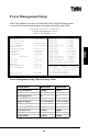
Chipset Features Setup
This section describes features of the VIA Appollo Pro Plus 133A chipset.
Advanced Options
The parameters in this screen are for system designers, service personnel, and
technically competent users only. Do not reset these values unless you
understand the consequences of your changes. Note: This chapter describes
all fields offered by Award Software in this screen. Your system board designer
may omit or modify some fields.
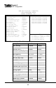
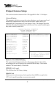
Bank 0/1 DRAM Timing : SDRAM 10ns Auto Detect DIMM/PCI Clk : Enabled
Bank 2/3 DRAM Timing : SDRAM 10ns CPU Clock/Spread Spectrum: Default
Bank 4/5 DRAM Timing : SDRAM 10ns
SDRAM Cycle Length : 3
DRAM Clock : HCLK -33M
Memory Hole : Disabled
P2C/C2P Concurrency : Enabled
Fast R-W Turnaround : Disabled
CPU IOQ Size : 1 Level
System BIOS Cacheable : Enabled
Video RAM Cacheable : Enabled
AGP Aperture Size : 64M
AGP Driving Control : Manual
AGP Driving Value : EC
AGP-4x Mode : Enabled
OnChip USB : Enabled
USB Keyboard Support : Disabled
Bank 0/1, 2/3, 4/5 DRAM Timing
The system board designer must select the proper value for these fields,
according to the specifications of the installed DRAM chips. Turbo mode
reduces CAS access time by 1 clock tick.
SDRAM Cycle Length
This field sets the CAS latency timing.
DRAM Clock
Allows you to set the memory clock speed to either 66MHz or equal to the
CPU clock speed, depending on your memory speed.
ROM PCI/ISA BIOS (TYAN1854)
CHIPSET FEATURES SETUP
AWARD SOFTWARE, INC.
ESC :Quit ↑↓ →← : Select Item
F1 : Help PU/PD/+/- : Modify
F5 : Old Values (Shift)F2 : Color
F6 : Load BIOS Defaults
F7 : Load Setup Defaults