JODY-W1 series Host-based multiradio modules with Wi-Fi and Bluetooth Data Sheet Abstract This technical data sheet describes the JODY-W1 series modules with 2x2 MIMO 802.11n/ac and dual-mode Bluetooth® v4.2. JODY-W1 is ideal for in-vehicle-infotainment and telematics applications with simultaneous use cases requiring high data rates, such as in-car hotspots, Wi-Fi display applications such as Apple CarPlay, or video streaming across multiple clients.
JODY-W1 series - Data Sheet Document Information Title JODY-W1 series Subtitle Host-based multiradio modules with Wi-Fi and Bluetooth Document type Data Sheet Document number UBX-16013635 Revision and date R13 Disclosure Restriction Confidential 19-Mar-2019 Product status Corresponding content status Functional Sample Draft For functional testing. Revised and supplementary data will be published later. In Development / Prototype Objective Specification Target values.
JODY-W1 series - Data Sheet Contents Document Information ................................................................................................................................ 2 Contents .......................................................................................................................................................... 3 1 Functional description ......................................................................................................................... 5 1.
JODY-W1 series - Data Sheet 4.6.2 Wi-Fi ....................................................................................................................................................29 4.7 LTE Coexistence performance ...............................................................................................................30 4.7.1 Wi-Fi receiver performance with LTE coexistence filter ..........................................................30 4.7.
JODY-W1 series - Data Sheet 1 Functional description 1.1 Overview The JODY-W1 series is a compact module based on the Cypress CYW88359 and CYW89359 AEC-Q100 compliant chipsets. It enables Wi-Fi, Bluetooth®, and Bluetooth low energy communication, and is thus ideal for in-vehicle-infotainment and telematics applications with simultaneous use cases requiring high data rates, such as in-car hotspots, Wi-Fi display applications such as Apple CarPlay, or video streaming across multiple clients.
JODY-W1 series - Data Sheet 1.3 Product features Table 1: Key features of JODY-W1 series 1.4 Product description Model Description JODY-W163-A Automotive grade module with 2 antenna pins, RSDB mode with a single antenna pin. Support for SDIO host interface only. JODY-W164-A Automotive grade module with 2 antenna pins, RSDB mode with a single antenna pin. Support for PCIe host interface, except JODY-W164-07A-01.
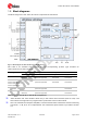
JODY-W1 series - Data Sheet 1.5 Block diagrams The block diagrams of the JODY-W1 series are provided in this section. Figure 1: Block diagram of JODY-W163-A and JODY-W164-A See Table 3 for available configurations and the corresponding product type numbers for JODY-W163-A and JODY-W164-A. Product type Antenna configuration Band-pass filters ANT0 ANT1 BPF_1 BPF_2 JODY-W164-03A-01 5 GHz Wi-Fi and Bluetooth 2.
JODY-W1 series - Data Sheet Figure 2: Block diagram of JODY-W167 (-A) 1.6 Wi-Fi operation modes This section lists the Wi-Fi operation modes supported by the dual-MAC architecture of the JODY-W1 series modules. The modules support Wi-Fi operation on two fully concurrent 1x1 SISO channels in RSDB configuration, or on a single channel in 2x2 MIMO configuration. Dual-mode Bluetooth is supported concurrently to the Wi-Fi operation mode. 1.6.1 RSDB single and multi-role operation modes 2.
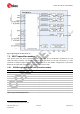
JODY-W1 series - Data Sheet 1.6.2 MIMO single and multi-role operation modes 2.4 GHz band 5 GHz band Notes AP Any channel STA Any channel P2P (GO) Any channel1 P2P (GC) Any channel AP+STA Any channel. AP+STA on the same 2.4 GHz channel. P2P (GO)+STA Any channel. P2P (GO)+STA on the same 2.4 GHz channel. P2P (GC)+STA Any channel. P2P (GC)+STA on the same 2.4 GHz channel. AP Any channel STA Any channel P2P (GO) Any channel1 P2P (GC) Any channel AP+STA Any channel.
JODY-W1 series - Data Sheet • MWS/LTE coexistence serial transport interface to connect an external and co-located LTE device 1.7.3 General product features • • • • • Driver support for Linux 3.x/4.x Low-power and sleep modes for Bluetooth and Wi-Fi core Coexistence arbitration for Wi-Fi/Bluetooth/LE/LTE operation Small footprint (19.8 mm x 13.8 mm), LGA package Automotive qualification tests (climatic, mechanical, and operating life tests) according ISO 16750-4 planned 1.7.
JODY-W1 series - Data Sheet 2 Interfaces 2.1 Host interface configuration JODY-W1 series module uses the Pin 6, Pin 7, and Pin 8 pins as host interface configuration input to set the desired operation mode following a reset. When you need to configure the pins for a certain module operation mode, you need to provide a 10 kΩ or less pull down resistor to the ground. No external circuitry is required to set a configuration pin to high logical level.
JODY-W1 series - Data Sheet 2.2.1 Default speed and High speed modes fPP tWL tWH SDIO_CLK tTHL tTLH tISU tIH INPUT tODLY tODLY (max) (min) OUTPUT Figure 3: SDIO Protocol timing diagram- Default speed mode (3.3 V) fPP tWL 50% VCC tWH SDIO_CLK tTHL tTLH tISU tIH INPUT tODLY tOH OUTPUT Figure 4: SDIO Protocol timing diagram – High speed mode (3.3 V) Symbol Parameter Condition Min. Typ Max.
JODY-W1 series - Data Sheet 2.2.2 SDR12, SDR25, SDR50 Modes (up to 100 MHz) (1.8 V) Figure 5: SDIO Protocol timing diagram – SDR12, SDR25, SDR50 modes (up to 100 MHz) (1.8 V) Symbol Parameter Condition Min. Typ Max. Units fPP Clock frequency SDR12 0 - 25 MHz SDR25 0 - 50 MHz SDR50 0 - 100 MHz SDR12/25/50 3 - - ns tIS Input setup time tIH Input hold time SDR12/25/50 0.
JODY-W1 series - Data Sheet Symbol Parameter Condition Min. 4.8 TCLK Clock time SDR104 tCR, tCF, Rise time, fall time TCR, TCF < 0.96 ns (max) at 208 MHz CCARD = 10 pF SDR104 TOP Card output phase SDR104 0 dTOP Delay variation due to temperature change after tuning SDR104 -350 TODW Output timing of variable data window SDR104 0.6 Typ Max. Units - - ns - 0.2*TCLK ns - 2 UI +1550 ps - - UI Table 10: SDIO Timing data – SDR104 mode (208 MHz) 2.2.4 DDR50 Mode (50 MHz) (1.
JODY-W1 series - Data Sheet Symbol Parameter Condition Min. Typ Max. Units tODLY Output delay time during data transfer mode CL ≤ 30 pF (1 card) DDR50 - - 13.7 ns tOHLD Output hold time CL ≥ 15 pF (1 card) DDR50 1.5 - - ns DAT[3:0] Input (referenced to clock rising and falling edges) tIS2x Input setup time CCARD ≤ 10 pF (1 card) DDR50 3 ns tIH2x Input hold time CCARD ≤ 10 pF (1 card) DDR50 0.
JODY-W1 series - Data Sheet Parameter Symbol Comments Min. Typ (2.5 GT/s) 0.15 (5 GT/s) Max. Units - RX detection voltage swing VTX-RCV-DETECT The amount of voltage change allowed during receiver detection - 600 mV TX AC peak commonmode voltage (5 GT/s) VTX-CM-AC-PP TX AC common mode voltage (2.5 GT/s) - - 100 mV TX AC peak commonVTX-CM-AC-P mode voltage (2.
JODY-W1 series - Data Sheet Baud Rate 9600 115200 (default) 1000000 2100000 19200 230400 1382400 2764800 38400 460800 1500000 3000000 57600 500000 1843200 3250000 76800 921600 2000000 3692300 4000000 Table 13: Supported UART Baud rates Figure 9: UART Timing Reference Characteristic Min. Typ Max. Units 1 Delay time, BT_UART_CTS low to BT_UART_TX valid - - 1.5 Bit period 2 Setup time, BT_UART_CTS high before midpoint of stop bit - - 0.
JODY-W1 series - Data Sheet 2.5.1 PCM Interface specifications Figure 10: PCM Timing specification – Short Frame Sync., Master mode Symbol Parameter Condition Min. Typ Max.
JODY-W1 series - Data Sheet Figure 11: PCM Timing specification – Short Frame Sync., Slave mode Symbol Parameter Condition Min. Typ Max.
JODY-W1 series - Data Sheet Symbol Parameter Condition Min. Typ Max. Units 1 PCM clock frequency - - - 12 MHz 2 PCM bit clock LOW - 41 - - ns 3 PCM bit clock HIGH - 41 - - ns 4 PCM_SYNC delay - 0 - 25 ns 5 PCM_OUT delay - 0 - 25 ns 6 PCM_IN setup - 8 - - ns 7 PCM_IN hold - 8 - - ns 8 Delay from rising edge of PCM_CLK during last bit period to PCM_OUT becoming high impedance - 0 - 25 ns Typ Max.
JODY-W1 series - Data Sheet Figure 14: PCM Burst mode timing specification – Short Frame Sync., Receiver only Symbol Parameter Condition Min. Typ Max. Units 1 PCM clock frequency - - - 24 MHz 2 PCM bit clock LOW - 20.8 - - ns 3 PCM bit clock HIGH - 20.8 - - ns 4 PCM_SYNC setup - 5 PCM_SYNC hold 6 PCM_IN setup 7 PCM_IN hold 8 - - ns 8 - - ns - 8 - - ns - 8 - - ns Table 19: PCM Burst mode timing specification – Short Frame Sync.
JODY-W1 series - Data Sheet The JODY-W1 series modules support I2S interface that provides clock rate in master mode 1.536 MHz (32 bits per frame) or 2.400 MHz (50 bits per frame). This interface is addressable over the PCM pins, which can be routed to the I²S interface through HCI commands.
JODY-W1 series - Data Sheet Parameter Transmitter Clock Period T Receiver Notes Lower Limit Upper Limit Lower Limit Upper Limit Min. Max. Min. Max. Min. Max. Min. Max. Ttr - - - Ttr - - T a Master Mode: Clock generated by transmitter or receiver HIGH tHC 0.35Ttr - - - 0.35Ttr - - - b Low tLC 0.35Ttr - - - 0.35Ttr - - - b Slave Mode: Clock accepted by transmitter or receiver HIGH tHC - 0.35Ttr - - - 0.35Ttr - - c Low tLC - 0.35Ttr - - - 0.
JODY-W1 series - Data Sheet 3 Pin definition 3.1 Pin description Figure 18: Pin assignment (top view) Power Supply Domain No. Name Pin Type Description 1 GND Ground Ground 2 VBAT Power 3.2 V < VBAT < 4.8 V 3 VIO Power VIO Supply (1.8 V or 3.3 V) 4 VIO_SD Power VIO Supply (1.8 V or 3.
JODY-W1 series - Data Sheet No. Name Pin Type Power Supply Domain Description De-asserted: Wi-Fi device may sleep when the sleep criteria is met 10 WL_HOST_WAKE O Wi-Fi HOST wake-up signal Asserted: Host device must wake-up or remain awake De-asserted: Host device may sleep when the sleep criteria is met VIO 11 BT_DEV_WAKE I Bluetooth device wake-up signal: Asserted: Bluetooth device must wake-up or remain awake De-asserted: Bluetooth device may sleep when sleep criteria are met.
JODY-W1 series - Data Sheet Power Supply Domain No.
JODY-W1 series - Data Sheet 4 Electrical specification B Stressing the device above one or more of the ratings listed in the Absolute Maximum Rating section may cause permanent damage. These are stress ratings only. Operating the module at these or at any conditions other than those specified in the Operating conditions section of this document should be avoided. Exposure to absolute maximum rating conditions for extended periods may affect device reliability.
JODY-W1 series - Data Sheet Table 25: DC characteristics SDIO digital I/O pins The following ratings are for all other digital I/O pins including GPIOs. Symbol Parameter VIO Min. Max. Units VIH Input high voltage 1.8 V 0.65*VIO - V 3.3 V 2.0 - V 1.8 V - 0.35*VIO V 3.3 V - 0.8 V 1.8 V VIO-0.45 - V 3.3 V VIO-0.4 - V 1.8 V - 0.45 V 3.3 V - 0.
JODY-W1 series - Data Sheet Table 28: Current consumption for Wi-Fi power-save modes at 25 °C 4.5 Bluetooth power consumption Operation mode: Bluetooth mode with Wi-Fi powered down Typical VBAT (3.3 V) current, µA Typical VIO (1.8 V) current, µA Typical VIO (3.3 V) current, µA Sleep 5.3 130 170 Standard 1.
JODY-W1 series - Data Sheet Parameter Operation Mode Specification RF Frequency range 802.11b/g/n 2.400 – 2.500 GHz 802.11a/n/ac 4.900 – 5.845 GHz 802.11b CCK and DSSS 802.11a/g/n/ac OFDM 802.11b 1, 2, 5.5, 11 Mbps 802.11a/g 6, 9, 12, 18, 24, 36, 48, 54 Mbps 802.11n SISO MCS0 - MCS7 (150 Mbps) Modulation Supported data rates 802.11n MIMO MCS8 – MCS15 (300 Mbps) 802.11ac SISO MCS0 – MCS9 (433 Mbps) 802.11ac MIMO MCS0 – MCS9 (867 Mbps) Supported channel bandwidth 2.
JODY-W1 series - Data Sheet LTE Band 7, 38, 41 Wi-Fi Sensitivity with presence of LTE Interferer Coexistence BPF DSS/CCK 1Mbps LTE Band 40 Wi-Fi Sensitivity with presence of LTE Interferer Coexistence BPF DSS/CCK 1Mbps -30 -20 -10 -50 0 -40 LTE Interferer Power (dBm) -30 -20 -10 0 -10 -10 -20 -20 -30 -40 -50 -60 -30 -40 -50 -60 -70 -70 -80 -80 -90 -90 Ch 1 2510 MHz Ch7 2510 MHz -100 Ch 13 2510 MHz Ch 1 2350 MHz Ch 7 2350 MHz -100 Ch 13 2350 MHz Ch 1 2530 MHz Ch 7 2530 MHz Ch 1
JODY-W1 series - Data Sheet LTE Band 40 Wi-Fi Sensitivity with presence of LTE Interferer Ordinary BPF DSS/CCK 1Mbps LTE Band 7, 38, 41 Wi-Fi Sensitivity with presence of LTE Interferer Ordinary BPF DSS/CCK 1Mbps LTE Interferer Power (dBm) -20 -10 -50 0 -40 -30 -20 -10 0 0 0 -10 -10 -20 -30 -40 -50 -60 -20 -30 -40 -50 -60 -70 -70 -80 -80 -90 -90 -100 -100 Ch1 2350 MHz Ch 7 2350 MHz Ch 13 2350 MHz Ch 1 2510 MHz Ch 7 2510 MHz Ch 13 2510 MHz Ch 1 2370 MHz Ch 7 2370 MHz Ch 13 237
JODY-W1 series - Data Sheet Symbol Parameter Condition Value Units θJA Junction to ambient thermal resistance θJA = (TJ - TA) / PH TJ = Junction temperature TA = Ambient temperature PH = Dissipated power from device JESD51-2A JEDEC 2S2P board inside thermal chamber, No air flow 19.4 °C/W ΨJT Junction to top of package thermal characterization parameter θJA = (TJ – TT) / PH TT = Top of package temperature JESD51-2A JEDEC 2S2P board inside thermal chamber, No air flow 13.
JODY-W1 series - Data Sheet 5 Host drivers and firmware 5.1 General principle The JODY-W1 series module does not contain any persistent software. A firmware binary will be downloaded by the host operating system driver on system start-up. Separate driver packages, including the firmware binaries, are available for PCIe and SDIO Wi-Fi host interface operation. 5.2 Supported operating systems 5.2.1 Linux Linux device drivers are available free of charge from the chipset manufacturer.
JODY-W1 series - Data Sheet 6 Mechanical specifications Pin1 M H F Keep this area free of copper* J O O L J Keep this area free of copper* H G E D D A * Seating Future module variants can have more pins in this area. To ensure compatibility this area should be kept free of copper. ccc Plane Figure 19: JODY-W1 series dimensions (bottom view) Parameter Description Typical Tolerance A Module Length [mm] 19.8 (779.5 mil) +0.35/-0.1 (+13.8/-3.9 mil) B Module Width [mm] 13.
JODY-W1 series - Data Sheet 7 Approvals The JODY-W1 series modules comply with the regulatory demands of Federal Communications Commission (FCC), Industry Canada (IC) and the CE mark5. B See JODY-W1 series System Integration Manual [2] for detailed information about regulatory compliance requirements of end products that use JODY-W1 series module. 7.
JODY-W1 series - Data Sheet 7.3.
JODY-W1 series - Data Sheet 7.3.3 ISED compliance statement The JODY-W1 series module complies with ISED (Innovation, Science and Economic Development Canada)9 license-exempt RSSs. Operation is subject to the following two conditions: (1) This device may not cause interference, and (2) This device must accept any interference, including interference that may cause undesired operation of the device.
JODY-W1 series - Data Sheet = Opération dans la bande 5600-5650 MHz n'est pas autorisée au Canada. Haute puissance radars sont désignés comme utilisateurs principaux (c.-àutilisateurs prioritaires) des bandes 52505350 MHz et 5650-5850 MHz et que ces radars pourraient causer des interférences et / ou des dommages à dispositifs LAN-EL. L’étiquette d’homologation d’ISED d’un module donné doit être posée sur l’appareil hôte à un endroit bien en vue en tout temps.
JODY-W1 series - Data Sheet 7.5.2 Bluetooth operation For Bluetooth operation, the JODY-W1 series module has been tested and approved for use with the antennas listed in Table 36. Manufacturer Part Number Antenna type Peak gain [dBi] Validated Regulatory Domain 2.4 GHz band 5 GHz band Any N/A Dipole antenna 2 2 FCC/IC Any N/A Dipole antenna 0 0 ETSI Table 36: List of approved Bluetooth antennas 7.
JODY-W1 series - Data Sheet 8 Product handling 8.1 Packaging The JODY-W1 series modules are delivered as hermetically sealed tape and reels, to enable efficient production, production lot set-up and tear-down. For more information about packaging, see the u-blox Package Information Guide [1]. 8.1.1 Reels The JODY-W1 series modules are deliverable in quantities of 500 pieces on a reel. The JODY-W1 series modules are shipped on reel Type A as described in the u-blox Package Information Guide [1]. 8.1.
JODY-W1 series - Data Sheet After opening the dry pack, the modules with MSL 3 must be mounted within 168 hours in factory conditions of maximum 30 °C/60%RH or must be stored at less than 10%RH. The modules with MSL 4 must be mounted within 72 hours. The modules require baking if the humidity indicator card shows more than 10% when read at 23±5°C or if the conditions mentioned above are not met. Please refer to J-STD-033B standard for the bake procedure. 8.2.
JODY-W1 series - Data Sheet 9 Labeling and ordering information 9.1 Product labeling The labels of JODY-W1 series include important product information as described in this section. The data matrix code for automotive and professional grade variants of JODY-W1 series includes a serial number. Figure 21 illustrates the sample label of the JODY-W1 series and includes: the u-blox logo, product name (model), type number, FCC and IC certification number and date of unit production encoded YY/WW (year/week).
JODY-W1 series - Data Sheet The product variant name, which is identical to the ordering code, used for product type approval is shown on the first line of the label. Table 38 provides the mapping of ordering code, label contents and FCC/ISED IDs. The marking “yy” in Reference 2 on the label is the minor product version and not relevant for certification.
JODY-W1 series - Data Sheet Ordering Code Product name Product JODY-W163-04A JODY-W163-A Automotive grade module based on CYW89359 transceiver, 2-antenna version, RSDB operation on a single antenna. No MIMO support. SDIO host interface. JODY-W163-05A JODY-W163-A Automotive grade module based on CYW88359 transceiver, 2-antenna version, RSDB operation on a single antenna. No MIMO support. SDIO host interface.
JODY-W1 series - Data Sheet Appendix A Glossary Abbreviation Definition AC Alternating Current BT Bluetooth CMD Command DC Direct Current DDR Double Data Rate ESD Electrostatic Sensitive Devices FCC Federal Communications Commission FIFO First In, First Out GI Guard interval GND Ground GPIO General-purpose input/output HD High Definition HCI Host Controller Interface ISED Innovation, Science and Economic Development Canada ISM Industrial, scientific and medical LE Low Energ
JODY-W1 series - Data Sheet Abbreviation Definition SDIO Secure Digital Input Output SDR Single Data Rate SISO Single-input single-output SMD Surface-mount Device STA Station TBD To be defined USB Universal Serial Bus UART Universal Asynchronous Receiver/Transmitter VSDB Virtual Simultaneous Dual Band WAPI WLAN Authentication and Privacy Infrastructure WLAN Wireless Local Area Network Table 42: Explanation of the abbreviations and terms used UBX-16013635 - R13 Confidential Appendi
JODY-W1 series - Data Sheet Related documents [1] [2] [3] [4] [5] = u-blox Package Information Guide, document number UBX-14001652 JODY-W1 series System Integration Manual, document number UBX-15024929 JODY-W1 antenna reference design, document number UBX-18017767 JODY-W1 reflow mounted upside down, Information Note, document number UBX-18021974 Radio Equipment Directive; ec.europa.
JODY-W1 series - Data Sheet Revision Date Name Comments Updated support of a single host interface only (SDIO or PCIe) per product variant. Updated the chipset information. Major updates in Approvals section (standards references, approved antennas, Bluetooth qualification). Added Table 38. Updated the current consumption for Wi-Fi power-save modes (Table 28). Added information on the permitted number of reflow processes for JODY-W164-04A and the reference to the related Information Note [4].
JODY-W1 series - Data Sheet Contact For complete contact information, visit us at www.u-blox.com. u-blox Offices North, Central and South America u-blox America, Inc. Phone: E-mail: +1 703 483 3180 info_us@u-blox.com Regional Office West Coast: Phone: E-mail: +1 408 573 3640 info_us@u-blox.com Headquarters Europe, Middle East, Africa Asia, Australia, Pacific u-blox AG Phone: +65 6734 3811 E-mail: info_ap@u-blox.com Support: support_ap@u-blox.com Phone: +41 44 722 74 44 E-mail: info@u-blox.