
Data Sheet


JODY-W1 series - Data Sheet
UBX-16013635 - R13 Contents Page 25 of 50
Confidential
. . '"#$ $
'$$#
De
-
asserted: Wi
-
Fi device may sleep
when the sleep criteria is met
10 WL_HOST_WAKE
O Wi-Fi HOST wake-up signal
Asserted: Host device must wake-up or remain awake
De-asserted: Host device may sleep when the sleep criteria is met
VIO
11 BT_DEV_WAKE I Bluetooth device wake-up signal:
Asserted: Bluetooth device must wake-up or remain awake
De-asserted: Bluetooth device may sleep when sleep criteria are met.
VIO
12 BT_HOST_WAKE O Bluetooth Host wake-up signal:
Asserted: Host device must wake-up or remain awake
De-asserted: Host device may sleep when sleep criteria are met
VIO
13 LTE_COEX_TX O Coexistence WCI2 interface. TX signal VIO
14 LTE_COEX_RX I Coexistence WCI2 interface. RX signal VIO
15 PCM_SYNC I/O PCM sync, can be output (master) or input (slave) VIO
16 PCM_CLK I/O PCM clock, can be output (master) or input (slave) VIO
17 PCM_OUT O PCM data output VIO
18 PCM_IN I PCM data input VIO
19 GND Ground Ground
20 GND Ground Ground
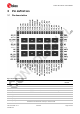
21 ANT2 I/O, RF Antenna pin (refer to section 1.5 Block diagrams)
22 GND Ground Ground
23 GND Ground Ground
24 ANT0 I/O, RF Antenna pin (refer to section 1.5 Block diagrams)
25 GND Ground Ground
26 NC - Reserved antenna pin. Do not connect.
27 GND Ground Ground
28 GND Ground Ground
29 ANT1 I/O, RF Antenna pin (refer to section 1.5 Block diagrams)
30 GND Ground Ground
31 GND Ground Ground
32 I2S_DI I/O
Reserved for I²S interface. Do not connect!
To connect a I²S interface the PCM pins can be used. The PCM
interface can be configured as an I²S interface. See chapter 2.5 for
more information.
VIO
33 I2S_DO I/O VIO
34 I2S_CLK I/O VIO
35 I2S_WS I/O VIO
36 BT_UART_TX O Fast UART serial data output for the Bluetooth device VIO
37 BT_UART_RX I Fast UART serial data input for the Bluetooth device VIO
38 BT_UART_RTS O Fast UART active-low request-to-send signal for the Bluetooth device VIO
39 BT_UART_CTS I Fast UART active-low clear-to-send signal for the Bluetooth device VIO
40 PCIE_PME# OD PCI power management event output VIO_SD
41 PCIE_CLKREQ# OD PCIe clock request signal VIO_SD
42 PCIE_PERST# I PCIe System reset VIO_SD
43 PCIE_REFCLKN I
PCIe 100 MHz clock differential input, AC coupling capacitors 100 pF
included in the module.
44 PCIE_REFCLKP I
45 PCIE_RDN I
PCIe receiver differential input, DC coupled inputs, use 100 nF AC
coupling capacitors placed closer to the Host TDN/TDP differential
output
46 PCIE_RDP I