
Installation Instructions


LISA-U2 series - System Integration Manual
UBX-13001118 - R19 Early Production Information System description
Page 10 of 175
Power Management Unit with integrated DC/DC converter for the Power Amplifier Module
Voltage Controlled Temperature Compensated 26 MHz Crystal Oscillator (VC-TCXO)
While operating in 3G mode, the RF transceiver performs direct up-conversion and down-conversion of the
baseband I/Q signals, with the RF voltage controlled gain amplifier being used to set the uplink TX power. In the
downlink path, the integrated LNA enhances the RX sensitivity while discrete inter-stage SAW filters additionally
improve the rejection of out-of-band blockers. An internal programmable gain amplifier optimizes the signal
levels before delivering to the analog I/Q to baseband for further digital processing.
For 2G operations, a constant gain direct conversion receiver with integrated LNAs and highly linear RF
quadrature demodulator are used to provide the same I/Q signals to the baseband as well. In transmission mode,
the up-conversion is implemented by means of a digital sigma-delta transmitter or polar modulator depending
on the modulation to be transmitted.
The RF antenna pad for the diversity receiver (ANT_DIV) available on LISA-U230 modules is directly connected to
the antenna switch for the diversity receiver, which dispatches the incoming RF signals to the dedicated SAW
filter bank for out-of-band rejection and then to the diversity receiver port of the RF transceiver.
In all the modes, a fractional-N sigma-delta RF synthesizer and an on-chip 3.296-4.340 GHz voltage controlled
oscillator are used to generate the local oscillator signal. The frequency reference to RF oscillators is provided by
the 26 MHz VC-TCXO. The same signal is buffered to the baseband as a master reference for clock generation
circuits while operating in active mode.
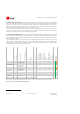
LISA-U2 series modulation techniques
Modulation techniques related to radio technologies supported by LISA-U2 modules, are listed as follows:
GSM GMSK
GPRS GMSK
EDGE GMSK / 8-PSK
WCDMA QPSK
HSDPA QPSK / 16-QAM
HSUPA QPSK / 16-QAM
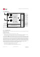
LISA-U2 series Baseband and Power Management Unit section
Another shielding box of LISA-U2 modules includes all the digital circuitry and the power supplies, basically the
following functional blocks:
Cellular baseband processor, a mixed signal ASIC which integrates:
Microprocessor for controller functions, 2G & 3G upper layer software
DSP core for 2G Layer 1 and audio processing
3G coprocessor and HW accelerator for 3G Layer 1 control software and routines
Dedicated HW for interfaces management
Memory system in a Multi-Chip Package (MCP) integrating two devices:
NOR flash non-volatile memory
DDR SRAM volatile memory
Power Management Unit (PMU), used to derive all the system supply voltages from the module supply VCC
32.768 kHz crystal, connected to the Real Time Clock (RTC) oscillator to provide the clock reference in idle or
power-off mode