
Integration Manual


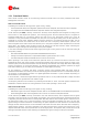
Table Of Contents
- Preface
- Contents
- 1 System description
- 1.1 Overview
- 1.2 Architecture
- 1.3 Pin-out
- 1.4 Operating modes
- 1.5 Power management
- 1.6 System functions
- 1.7 RF connection
- 1.8 (U)SIM interface
- 1.9 Serial communication
- 1.10 DDC (I2C) interface
- 1.11 Audio Interface
- 1.12 General Purpose Input/Output (GPIO)
- 1.13 Reserved pins (RSVD)
- 1.14 Schematic for LISA-U series module integration
- 1.15 Approvals
- 2 Design-In
- 2.1 Design-in checklist
- 2.2 Design Guidelines for Layout
- 2.2.1 Layout guidelines per pin function
- 2.2.2 Footprint and paste mask
- 2.2.3 Placement
- 2.3 Thermal aspects
- 2.4 Antenna guidelines
- 2.5 ESD precautions
- 3 Features description
- 4 Handling and soldering
- 5 Product Testing
- Appendix
- A Migration to LISA-U2 series wireless modules
- B Glossary
- Related documents
- Revision history
- Contact

LISA-U series - System Integration Manual
3G.G2-HW-10002-A3 Preliminary System description
Page 9 of 160
1.2 Architecture
Wireless
Base-band
Processor
Memory
Power Management Unit
RF
Transceiver
26 MHz
32.768 kHz
SAW
Filter
FEM & 2G PA
ANT
LNA
3G PA
LNA
3G PA
DDC (for GPS)
(U)SIM Card
UART
SPI
USB
GPIO(s)
Power On
External Reset
V_BCKP (RTC)
Vcc (Supply)
V_INT (I/O)
Digital Audio (I
2
S)
AnalogAudio
Figure 1: LISA-U1 series block diagram (for available options refer to the product features summary in Table 2)
Wireless
Base-band
Processor
Memory
Power Management Unit
26 MHz
32.768 kHz
ANT
Switch & Multi band & mode PA
DDC (for GPS)
(U)SIM Card
UART
SPI
USB
GPIO(s)
Power On
External Reset
V_BCKP (RTC)
Vcc (Supply)
V_INT (I/O)
Digital Audio (I
2
S)
RF
SWITCH
RF
Transceiver
Duplexers
& Filters
ANT_DIV
RF
SWITCH
Filter
Bank
PA
PMU
Transceiver
PMU
Figure 2: LISA-U2 series block diagram (for available options refer to the product features summary in Table 2)