
Data Sheet


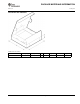

Top View
Clearance area.
Keep free of any
conductive materials.
Device
LEGEND
Top layer; copper pour and traces
High-side area
Controller-side area
Via
To Shunt
To Filter or ADC
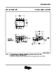
VDD1
VINP
GND1
VINN
VDD2
VOUTP
VOUTN
GND2
0.1mF
SMD
1206
0.1 F
SMD
1206
m
0.1 F
SMD
1206
m
330 pF
SMD
0603
12
SMD 0603
W
12
SMD 0603
W
AMC1100
www.ti.com
SBAS562 –APRIL 2012
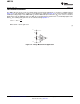
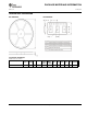
As shown in Figure 33, it is recommended to place the bypass and filter capacitors as close as possible to the AMC1100 to ensure best performance.
Figure 33. AMC1100 Layout Recommendation
To maintain the isolation barrier and the common-mode transient immunity (CMTI) of the device, the distance between the high-side ground (GND1) and
the low-side ground (GND2) should be kept at maximum; that is the entire area underneath the device should be kept free of any conducting materials.
Copyright © 2012, Texas Instruments Incorporated Submit Documentation Feedback 13
Product Folder Link(s): AMC1100