
Data Sheet


CAUTION: These devices are sensitive to electrostatic discharge. Users should follow proper I.C. Handling Procedures.
Copyright
© Harris Corporation 1992
7-1392
SEMICONDUCTOR
CD40175BMS
CMOS Quad ‘D’ Type Flip-Flop
Features
• High Voltage Type (20V Rating)
• Output Compatible with Two HTL Loads, Two Low Power
TTL Loads, or One Low Power Schottky TTL Load
• Functional Equivalent to TTL74175
• 100% Tested for Quiescent Current at 20V
• 5V, 10V and 15V Parametric Ratings
• Maximum Input Current of 1µA at 18V Over Full Pack-
age Temperature Range; 100nA at 18V and +25
o
C
• Noise Margin (Over Full Package/Temperature Range)
- 1V at VDD = 5V
- 2V at VDD = 10V
- 2.5V at VDD = 15V
• Standardized Symmetrical Output Characteristics
• Meets All Requirements of JEDEC Tentative Standard
No. 13B, “Standard Specifications for Description of
‘B’ Series CMOS Devices”
Applications
• Shift Registers
• Buffer/Storage Registers
• Pattern Generators
Description
CD40175BMS consists of four identical D-type flip-flops.
Each flip-flop has an independent DATA D input and comple-
mentary Q and
Q outputs. The CLOCK and CLEAR inputs
are common to all flip-flops. Data are transferred to the Q
outputs on the positive going transition of the clock pulse. All
four flip-flops are simultaneously reset by a low level on the
CLEAR input.
These devices can function as shift register elements or as
T-type flip-flops for toggle and counter applications.
The CD40175BMS is supplied in these 16-lead outline
packages:
Braze Seal DIP H4T
Ceramic Flatpack H6W
December 1992
File Number
3360
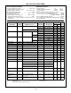
Pinout
CD40175BMS
TOP VIEW
Functional Diagram
14
15
16
9
13
12
11
10
1
2
3
4
5
7
6
8
CLEAR
Q1
Q1
D1
D2
Q2
VSS
Q2
VDD
Q4
D4
D3
Q3
Q3
CLOCK
Q4
VDD = PIN 16
VSS = PIN 8
F/F1
4
D1
2
3
Q1
Q1
F/F2
5
D2
7
6
Q2
Q2
F/F3
12
D3
10
11
Q3
Q3
F/F4
13
D4
15
14
Q4
Q4
9
CLOCK
1
CLEAR
VSS = 8
VDD = 16