
Data Sheet


1
Data sheet acquired from Harris Semiconductor
SCHS047G
CAUTION: These devices are sensitive to electrostatic discharge; follow proper IC Handling Procedures.
Copyright
© 2003, Texas Instruments Incorporated
CD4051B, CD4052B, CD4053B
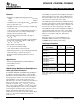
Features
• Wide Range of Digital and Analog Signal Levels
- Digital . . . . . . . . . . . . . . . . . . . . . . . . . . . . . . 3V to 20V
- Analog. . . . . . . . . . . . . . . . . . . . . . . . . . . . . . . ≤20V
P-P
• Low ON Resistance, 125Ω (Typ) Over 15V
P-P
Signal Input
Range for V
DD
-V
EE
= 18V
• High OFF Resistance, Channel Leakage of ±100pA (Typ)
at V
DD
-V
EE
= 18V
• Logic-Level Conversion for Digital Addressing Signals of
3V to 20V (V
DD
-V
SS
= 3V to 20V) to Switch Analog
Signals to 20V
P-P
(V
DD
-V
EE
= 20V)
• Matched Switch Characteristics, r
ON
= 5Ω (Typ) for
V
DD
-V
EE
= 15V
• Very Low Quiescent Power Dissipation Under All Digital-
Control Input and Supply Conditions, 0.2µW (Typ) at
V
DD
-V
SS
= V
DD
-V
EE
= 10V
• Binary Address Decoding on Chip
• 5V, 10V, and 15V Parametric Ratings
• 100% Tested for Quiescent Current at 20V
• Maximum Input Current of 1µA at 18V Over Full Package
Temperature Range, 100nA at 18V and 25
o
C
• Break-Before-Make Switching Eliminates Channel
Overlap
Applications
• Analog and Digital Multiplexing and Demultiplexing
• A/D and D/A Conversion
• Signal Gating
CMOS Analog Multiplexers/Demultiplexers
with Logic Level Conversion
The CD4051B, CD4052B, and CD4053B analog multiplexers
are digitally-controlled analog switches having low ON
impedance and very low OFF leakage current. Control of
analog signals up to 20V
P-P
can be achieved by digital
signal amplitudes of 4.5V to 20V (if V
DD
-V
SS
= 3V, a
V
DD
-V
EE
of up to 13V can be controlled; for V
DD
-V
EE
level
differences above 13V, a V
DD
-V
SS
of at least 4.5V is
required). For example, if V
DD
= +4.5V, V
SS
= 0V, and
V
EE
= -13.5V, analog signals from -13.5V to +4.5V can be
controlled by digital inputs of 0V to 5V. These multiplexer
circuits dissipate extremely low quiescent power over the
full V
DD
-V
SS
and V
DD
-V
EE
supply-voltage ranges,
independent of the logic state of the control signals. When
a logic “1” is present at the inhibit input terminal, all
channels are off.
The CD4051B is a single 8-Channel multiplexer having three
binary control inputs, A, B, and C, and an inhibit input. The
three binary signals select 1 of 8 channels to be turned on,
and connect one of the 8 inputs to the output.
The CD4052B is a differential 4-Channel multiplexer having
two binary control inputs, A and B, and an inhibit input. The
two binary input signals select 1 of 4 pairs of channels to be
turned on and connect the analog inputs to the outputs.
The CD4053B is a triple 2-Channel multiplexer having three
separate digital control inputs, A, B, and C, and an inhibit
input. Each control input selects one of a pair of channels
which are connected in a single-pole, double-throw
configuration.
When these devices are used as demultiplexers, the
“CHANNEL IN/OUT” terminals are the outputs and the
“COMMON OUT/IN” terminals are the inputs.
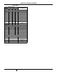
NOTE: When ordering, use the entire part number. The suffixes 96
and R denote tape and reel. The suffix T denotes a small-quantity
reel of 250.
Ordering Information
PART NUMBER
TEMP. RANGE
(
o
C) PACKAGE
CD4051BF3A, CD4052BF3A,
CD4053BF3A
-55 to 125 16 Ld CERAMIC
DIP
CD4051BE, CD4052BE,
CD4053BE
-55 to 125 16 Ld PDIP
CD4051BM, CD4051BMT,
CD4051BM96
CD4052BM, CD4052BMT,
CD4052BM96
CD4053BM, CD4053BMT,
CD4053BM96
-55 to 125 16 Ld SOIC
CD4051BNSR, CD4052BNSR,
CD4053BNSR
-55 to 125 16 Ld SOP
CD4051BPW, CD4051BPWR,
CD4052BPW, CD4052BPWR
CD4053BPW, CD4053BPWR
-55 to 125 16 Ld TSSOP
August 1998 - Revised October 2003
[ /Title
(CD405
1B,
CD4052
B,
CD4053
B)
/Sub-
ject
(CMOS
Analog
Multi-
plex-
ers/Dem
ultiplex-
ers with
Logic
Level
Conver-
sion)
/Author
()
/Key-
words
(Harris
Semi-
conduc-
tor,
CD4000