
Data Sheet


V
DD
1
2
3
4
5
6
7
8
16
15
14
13
12
11
10
9
1
2
3
4
5
6
7
8
16
15
14
13
12
11
10
9
1
2
3
4
5
6
7
8
16
15
14
13
12
11
10
9
I
DD
I
DD
I
DD
V
V
CD4053
DD
DD
CD4052
t = 20ns
f
10%
10%
90%
50%
10%
50%
90%
10%
50%
90%
t = 20ns
r
TURN-OFF TIME
TURN-ON TIME
t = 20ns
f
10%
90%
50%
10%
50%
90%
10%
90%
t = 20ns
r
TURN-OFF TIME
TURN-ON
t
PHZ
TIME
V = 5V
DD
V = 0V
SS
V = -7.5V
EE
7
8
(B)
(C)
(D)
(A)
V = 7.5V
DD
7.5V
1616 1616
7
8
7
8
V = 5V
DD
V = 15V
DD
V = 0V
SS
V = 0V
EE
7
8
5V
EE
V = -10V
V = 0V
SS
V = 0V
SS
5V
EE
V = -5V
11
CD4051B
,
CD4052B
,
CD4053B
www.ti.com
SCHS047I –AUGUST 1998–REVISED SEPTEMBER 2017
Product Folder Links: CD4051B CD4052B CD4053B
Submit Documentation FeedbackCopyright © 1998–2017, Texas Instruments Incorporated
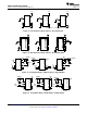
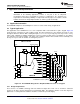
7 Parameter Measurement Information
Figure 9. Typical Bias Voltages
NOTE
The ADDRESS (digital-control inputs) and INHIBIT logic levels are: 0 = V
SS
and 1 = V
DD
. The analog signal (through the TG) may swing from V
EE
to V
DD
.
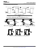
Figure 10. Waveforms, Channel Being Turned ON
(R
L
= 1 kΩ)
Figure 11. Waveforms, Channel Being Turned OFF
(R
L
= 1 kΩ)
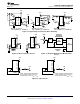
Figure 12. OFF Channel Leakage Current - Any Channel OFF