
Data Sheet
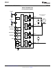
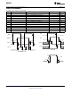
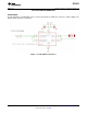

1
2
3
4
12
11
10
9
GND
(PPAD )
5 8
6 7
VM
AOUT1
AOUT2
BOUT1
BOUT2
GND
VCC
MODE
AIN1 / APHASE
AIN2 / AENBL
BIN1 / BPHASE
BIN2 / BENBL
DSS PACKAGE
(TOP VIEW)
DRV8835
www.ti.com
SLVSB18D –MARCH 2012–REVISED JANUARY 2014
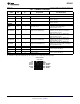
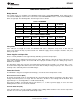
Table 1. TERMINAL FUNCTIONS
EXTERNAL COMPONENTS
NAME PIN I/O
(1)
DESCRIPTION
OR CONNECTIONS
POWER AND GROUND
GND 6 - Device ground
Bypass to GND with a 0.1-μF (minimum)
VM 1 - Motor supply
ceramic capacitor.
Bypass to GND with a 0.1-μF (minimum)
VCC 12 - Device supply
ceramic capacitor.
CONTROL
Logic low selects IN/IN mode.
MODE 11 I Input mode select Logic high selects PH/EN mode.
Internal pulldown resistor.
IN/IN mode: Logic high sets AOUT1 high.
AIN1/APHASE 10 I Bridge A input 1/PHASE input PH/EN mode: Sets direction of H-bridge A.
Internal pulldown resistor.
IN/IN mode: Logic high sets AOUT2 high.
AIN2/AENBL 9 I Bridge A input 2/ENABLE input PH/EN mode: Logic high enables H-bridge A.
Internal pulldown resistor.
IN/IN mode: Logic high sets BOUT1 high.
BIN1/BPHASE 8 I Bridge B input 1/PHASE input PH/EN mode: Sets direction of H-bridge B.
Internal pulldown resistor.
IN/IN mode: Logic high sets BOUT2 high.
BIN2/BENBL 7 I Bridge B input 2/ENABLE input PH/EN mode: Logic high enables H-bridge B.
Internal pulldown resistor.
OUTPUT
AOUT1 2 O Bridge A output 1
Connect to motor winding A
AOUT2 3 O Bridge A output 2
BOUT1 4 O Bridge B output 1
Connect to motor winding B
BOUT2 5 O Bridge B output 2
(1) Directions: I = input, O = output, OZ = tri-state output, OD = open-drain output, IO = input/output
Copyright © 2012–2014, Texas Instruments Incorporated Submit Documentation Feedback 3
Product Folder Links: DRV8835