L Z E G M B H • F R A U H E N W E I H E RS T R A S S E 1 5 • 9 1 0 5 8 E R L A N G E N FH3D02* DUAL 3D HALL SENSOR DATASHEET * Equivalent to FH5401c Seite 1 von 44 Copyright © 2021, LZE GmbH www.lze-innovation.
FH3D02 Overview Content 1 1.1 1.2 1.3 1.4 FH3D02 Overview ............................................................................................................. 4 General Description ........................................................................................................... 4 Features ............................................................................................................................. 4 Applications ............................................................
FH3D02 Overview 6.3.1 6.3.2 6.3.3 6.3.4 6.4 6.4.1 6.4.2 6.4.3 6.4.4 6.5 6.5.1 6.5.2 6.5.3 6.5.4 6.6 6.6.1 6.6.2 6.6.3 6.6.4 Application Example .......................................................................................................... 24 Settings .............................................................................................................................. 24 Output Registers ....................................................................................................
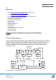
FH3D02 Overview 1 FH3D02 Overview 1.1 General Description The FH3D02 is a dual 3D magnetic field sensor using two 3D Hall sensors using the HallinOne® technology, which are also called “pixels”. The versatile magnetic field sensor is suited for measuring all magnetic field components in three dimensions. It can be used as a magnetic field probe or a position sensor for linear or rotary movement of permanent magnets. A variety of applications can be evaluated instantly with the standard programming.
FH3D02 Overview 1.3 Applications − − − − − − − − − − − − − − − 3D position and orientation determination (using multiple devices) o http://www.iis.fraunhofer.de/hallinmotion Magnetic field measurement in lab equipment o http://www.iis.fraunhofer.
Characteristics 2 Characteristics 2.1 Absolute Maximum Ratings Stresses beyond those listed here may cause permanent damage to the device. These are stress ratings only. Functional operation of the device at these or any other conditions beyond those indicated under “Operating Conditions” is not implied. Exposure to absolute maximum rating conditions for extended periods may affect device reliability. Parameter Min Max VDD Unit 5 V V Note Input pin voltage -0.3 VDD+0.
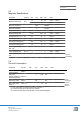
Characteristics 2.3 Magnetic Specifications Parameter Symbol Magnetic field range Bmax Min Typ Max Unit Note -70 70 mT -40°C … 105°C -100 100 mT at 25°C Magnetic sensitivity 250 LSB/mT Magnetic resolution 4 µT/LSB Magnetic offset Bofs Magnetic offset drift -0.25 0.25 mT at 25°C -0.25 0.25 mT -40°C … 105°C Sensitivity error X, Y, Z Serr -20 20 % at 25°C Sensitivity drift X, Y, Z Sdrift -5 5 % -40°C … 105°C Sensitivity matching X/Y -0.5 0.
Package and Circuit Connection 3 Package and Circuit Connection 3.
Package and Circuit Connection 3.2 Pins Pin Symbol Type A1 MISO DO_T A2 CLK A3 B3 VSS1 S A4 SCE DI_ST Test pin, must be connected to VSS in normal operation A5 LOPOW R DI_ST Shutdown & Reset input.
Package and Circuit Connection 3.3 Electrical Connection The sensor chip must be connected to a supply of 3.3V via its VDD and VSS pins. All unused pins should be connected to VSS to guarantee proper function. A decoupling capacitor between VDD and VSS close to the sensor chip is strongly recommended as well as the usage of non-magnetic components nearby to prevent magnetic interference.
SPI Communication 4 SPI Communication 4.1 Protocol and Timing The transferred data bits via MOSI (Master Out – Slave In) and MISO (Master In – Slave Out) are defined as follows: A15….A00 = 16-bit register address W15….W00 = 16-bit write data (in write mode) X15….
SPI Communication Output edge rise time Or 3 ns Output edge fall time Of 3 ns 4.2 Read/Write Access Data is transferred to the device via the MOSI pin with the rising edge of SCK. It should be updated by the master at the falling edge of SCK. Data is updated at the MISO pin with the falling edge of SCK and can safely be read from the device with the rising edge of SCK. The data format consists of data streams with 32 bit in length.
SPI Communication 4.2.3 CRC Calculation The CRC value in register 0x0108 is calculated as bitwise XOR operation of the SPI read data and the previous CRC value. It is recommended to implement an identical CRC calculation in the SPI master and compare the CRC value from register 0x0108 to the calculated value. Please note that the SPI command 0x0000 is regarded as read command, too. Hence its constant result of 0x8000 is also used for the CRC calculation.
List of Registers 5 List of Registers Following table shows all available registers for communication with the sensor via SIP. For detailed description of the register content and respective bit assignment go to the specified chapters. Register Read / Write Description Refer to chapter 0x0004 Read & Write Clock configuration register 7.6 0x000B Read & Write Measurement control register 5.1.1 0x000D Read PWM configuration register 7.4 0x000E Read & Write Measurement start register 5.1.
List of Registers 5.1 Measurement Register Contents 5.1.1 0x000B (read/write) – Measurement Control Bit Symbol Default Description D15 (MSB) r – D12 0 (Reserved. Always set to default state) D11 MgnRngExt 0 “Magnet Range Extension” Only useful if Bit Gradient = 1. Enables the algorithm for an extended position range. Refer to chapter 7.7 for further information.
List of Registers 5.1.2 0x000E (read/write) – Measurement Start Single shot measurements are started by SPI command 0x800E-0x0001. The last rising SCK edge triggers the measurement. The measurement completion is indicated by a READY rise. The same information is available as bit Ready of register 0x0107 (see section 5.1.3). It can be polled if connection of pin READY shall be omitted. READY is reset to logical 0 if register 0x0122 is read. A new measurement can be started now.
List of Registers Settling time Bit tres2 Symbol 200 Default µs Do not start a measurement before tres1+tres2! Description D15 (MSB) r – D2 0 (Reserved. Always set to default state) D1 ContMeas 0 “Continuous Measurement Enable” The measurement cycle is continuously repeated. After every measurement cycle the READY pin or flag (register 0x0107) is set. It must be reset during the next cycle to indicate the next cycle completion.
List of Registers 5.1.4 0x0110 (read only) – Temperature Sensor During every measurement cycle the internal temperature is measured sequentially with the magnetic values. The temperature value is used for internal compensation of magnetic sensor offsets and sensitivity drifts and is also available in output register 0x0110. Bit Symbol D15 (MSB) T – D0 (LSB) Description “Temperature” Output value of the internal temperature sensor. 16 bit signed integer value in two’s complement representation.
List of Registers 5.1.7 0x0113 (read only) – Bj0 Magnetic Field Depending on the table selection (Bits TableSelect in register 0x000B) the Bj0 output register can hold different magnetic field components. For an overview of the Bj0 contents refer to chapter 5.2. Bit Symbol D15 (MSB) Bj0 – D0 (LSB) Description “Bj0” Output value of magnetic field sensor. 16 bit signed integer value in two’s complement representation. For explanation of the real magnetic direction refer to chapter 5.2.
List of Registers 5.1.10 0x0121 (read only) – Magnetic Field Angle The CORDIC angle of the Bi and Bj field components is available in register 0x0121. In gradient mode the Bi and Bj differences are used as CORDIC input (see conversion formulas in the table). Bit Symbol D15 (MSB) angle – D0 (LSB) Description “angleB: CORDIC angle” CORDIC angle of Bi and Bj. 16 bit signed integer value in two’s complement representation.
List of Registers 5.2 Result Register Overview With different settings in the sequencer register 0x000B the FH3D02 can be used for various applications. Depending on the TableSelect settings in register 0x000B the results in registers 0x0111 – 0x0114, 0x0120 – 0x124 can hold different magnetic values. The following table gives an overview about the register content in different configurations. Register TableSelect 0b00 (1 kHz) TableSelect 0b01 (0.
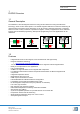
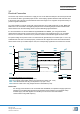
Measurement Modes 6 Measurement Modes 6.1 Single Magnetic Probe The three magnetic field components Bx0, By0 and Bz0 from pixel 0 can be measured in one measurement cycle by using the single probe mode. 6.1.1 Application Example Y X Z Magnetic vector components of Pixel 0 in probe mode. The actual sensors are placed at the bottom side of the IC. 6.1.
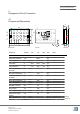
Measurement Modes 6.2 Dual Magnetic Probe All possible magnetic field components can be measured in one measurement cycle by using the dual probe mode. 6.2.1 Application Example Y X Z Magnetic vectors in dual probe mode. For exact pixel positions refer to chapter 3.1. 6.2.2 Settings Bit Setting 15 0 14 0 Default 0 0 Register 0x000B bit settings 13 0 12 0 11 0 10 0 9 1 8 1 7 0 6 1 5 0 4 0 3 0 2 0 1 Rdy2hZ 0 0 0 0 0 0 0 0 0 0 0 0 0 0 1 0 (1) 6.2.
Measurement Modes 6.3 Linear Position or Off-Axis Angle Sensor (Absolute Field Values, Magnet On-Top) With this setting a linear position measurement or an off-axis angle measurement is feasible. A linearization table can be used for both applications to allow for a linear output curve (see chapter 7.8). 6.3.1 Application Example Y X Z Pixel 0 Pixel 0 ball C1 ball C1 Magnet configuration examples in zero position 6.3.
Measurement Modes 6.4 Linear Position or Off-Axis Angle Sensor (Gradient Field Values, Magnet On-Top) With this setting a linear position measurement or an off-axis angle measurement is feasible. The gradient mode makes the angle value independent from homogeneous external fields. A linearization table can be used for both applications to allow for a linear output curve (see chapter 7.8). 6.4.
Measurement Modes 6.5 Linear Position or Off-Axis Angle Sensor (Absolute Field Values, Magnet At-The-Side) With this setting a linear position measurement or an off-axis angle measurement is feasible. A linearization table can be used for both applications to allow for a linear output curve (see chapter 7.8). 6.5.1 Application Example Pixel 0 Pixel 0 FH3D02 XXXX FH3D02 XXXX Y X Z Magnet configuration examples in zero position 6.5.
Measurement Modes 6.6 Linear Position or Off-Axis Angle Sensor (Gradient Field Values, Magnet At-The-Side) With this setting a linear position measurement or an off-axis angle measurement is feasible. The gradient mode makes the angle value independent from homogeneous external fields. A linearization table can be used for both applications to allow for a linear output curve (see chapter 7.8). 6.6.
Additional Features 7 Additional Features 7.1 Low Power Mode For low power applications the FH3D02 can be set to a low power mode. In this mode all analog components are turned off and the oscillator and digital components are stopped. The low power mode is enabled by logical levels at pin LOPOWR. A logical rise signal will immediately enable the low power mode. Any measurement will be interrupted and the SPI will not return any data.
Additional Features 7.2 EEPROM Access The internal 512 x 16bit EEPROM is a non-volatile memory which holds initialization and calibration data and the definition of internal measurement sequences. Certain address ranges of the EEPROM are accessible and can be modified. Others must not or can not be modified. Read and write access is performed via the SPI registers 0x0030 and 0x0031. The desired address is written to register 0030h and the stored bits can be read from register 0031h or written to it.
Additional Features The following table gives an overview about the content of different address ranges in the EEPROM. Address range Content Note 0x001 – 0x00F At the reset cycle the content of this EEPROM address range is copied to the SPI accessible SPI register initialization volatile memory and will be used during normal operation. 0x010 – 0x01F Sensor calibration data Do not access this address range.
Additional Features 7.3 EEPROM Access Restriction (Lock Modes) The lock mode definition at EEPROM address 0x020 can be used to prevent write and read access to the EEPROM. After setting single bits in the lock mode word and performing a reset cycle the bits can not be set back to 0. The following table gives an overview about the locked EEPROM functions and address ranges.
Additional Features D1 - 0 0 Reserved D0 (LSB) - 0 1 Read protection for measurement sequence definitions, linearization table, SPI register initialization. Recommended lock word for application: 0xD7FD Seite 32 von 44 Copyright © 2021, LZE GmbH www.lze-innovation.
Additional Features 7.4 PWM Output From the measured and linearized angle in SPI register 0x0122 a PWM signal can be generated. The base frequency of the PWM is the system clock frequency of typ. 8 MHz. Hence one PWM digit always corresponds to approx. 125 ns. The PWM signal is available at pin PWM. If one of the error flags MgnLost or CalcErr occurs the PWM output will be disabled with PWM remaining at the current level (high or low).
Additional Features t1 t2 … PWM … t = 1/f PWM t = 1/ fPWM t = 1/ fPWM 0% PWM Duty Cycle 50% 100% Timing diagram of 3 PWM cycles. t1/t and t2/t define the duty cycle. The last cycle represents an error state at which no PWM edge is generated. -32767 0 LinAngle [LSB] 32767 Characteristic curve of the PWM duty cycle vs linearized angle value. The black line represents the maximum possible PWM range. The green curve shows limited min and max values.
Additional Features 7.5 Parallel Operation of Multiple Devices For several applications it might be necessary to use several devices with only one master controller. The simplest way to communicate with several ICs for combined operation is to use separate CS_N wires for every device. Communication with a device is only possible while CS_N is low. Then the output MISO is active, otherwise it is high impedance (see also 4.1).
Additional Features Parameter Symbol Min Typ Clock frequency fclkExt 7.5 Edge rise time trise ns 0.3 V to 2.7 V Edge fall time tfall ns 2.7 V to 0.3 V Duty cycle tcduty 49 Max Unit 8 MHz 51 Note External clock characteristics % The clock behavior can be set by setting bits D10 and D11 in SPI register 0x0004. Bit Symbol D15 (MSB) r – D12 D11 OscOut Default Description Value 0 (Reserved.
Additional Features Please note: It is strongly recommended to use an impedance controlled digital signal line with source resistor (e.g. Rser as shown) for the clock wire. The reset sequence always uses the internal clock, even if 0x0440 is written to 0x0004 in the EEPROM. For synchronization reasons the external clock will not be used until the first SCK edge. This edge must not occur before the end of the reset cycle and does not need a CS_N=0.
Additional Features EEPROM Clock Settings If the oscillator settings from SPI register 0x0004 are stored in the EEPROM attention should be paid to the startup procedure: During the boot procedure an untrimmed internal clock frequency is used. After a certain time tres the rising READY indicates that the boot procedure is finished and communication on the SPI can commence.
Additional Features 7.7 Range Extension in Gradient Mode In any position sensing application an angle value is calculated from two magnetic components Bi and Bj. In rotary and absolute linear applications this angle can vary between +/-180° (see the graph below). For linear magnet movements the magnetic fields become lower at the outside of the movement range. The angle will be correct inside its limits until offsets and noise exceed the magnetic field amplitude. The linearization is properly applicable.
Additional Features Register values vs Position (gradient mode) 32768 24576 16384 Value [LSB] 8192 -10 -05 0 00 05 10 -8192 -16384 -24576 -32768 Position [mm] 0x111 (Bi0) 0x114 (Bj1) 0x112 (Bi1) 0x121 Gradient 0x113 (Bj0) 0x121 MgnRngExt Example data of real magnet in gradient mode. The standard CORDIC angle “Gradient” jumps between +/-180° if the Bj component crosses 0. “MgnRngExt” shows a valid angle without ambiguity by offering a range of +/-288°.
Additional Features 7.8 Linearization Table A linearized angle LinAngle (register 0x0122) is calculated from the direct CORDIC angle (0x0120) and a static linearization table in the EEPROM. The factory setting is a transparent table where 0x0122 holds the identical content as 0x0120. - 33 base points from -16 to +16 constant x distance of 2048 digits ( 11.
Additional Features - Record angle data vs movement with the used magnet/IC pair. Chose proper factor for movement quantization. (e.g. 2048 LSB/mm for this example) Invert the angle curve using this factor. Extrapolate the curve to generate (at least) the adjacent base points outside the existing data. Interpolate at base points and clip the curve to +/-32767. This linearization corrects for linearity errors and zero point offsets.
Additional Features 7.9 Magnet Lost Setting At every measurement the magnetic field magnitude is compared to an adjustable value and the flag MagLost in register 0x0107 is set if the magnitude falls below this value. In order to avoid a toggling flag on the edge of this limit a hysteresis can be set. Bit Symbol Description D15 – D11 r (Reserved. Always 0) D10 – D8 Hyst “Hysteresis” Hysteresis around the Magnet Lost Limit.
LZE GmbH 8 LZE GmbH LZE GmbH Geschäftsführer: Dr. Christian Forster Frauenweiherstr. 15 91058 Erlangen Kontakt Telefon: +49 9131 92894 80 E-Mail: contact[at]lze-innovation.de Umsatzsteuer-Identifikationsnummer gem. § 27 a Umsatzsteuergesetz: DE316405780 Handelsregisternummer: HRB 16647 Zuständiges Amtsgericht: Fürth * Ende des Dokuments * Seite 44 von 44 Copyright © 2021, LZE GmbH www.lze-innovation.