
Data Sheet
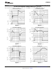
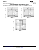

LP2985-N
SNVS018V –MARCH 2000–REVISED JUNE 2013
www.ti.com
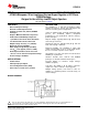
BASIC APPLICATION CIRCUIT
*ON/OFF input must be actively terminated. Tie to V
IN
if this function is not to be used.
**Minimum capacitance is shown to ensure stability (may be increased without limit). Ceramic capacitor required for
output (see APPLICATION HINTS).
***Reduces output noise (may be omitted if application is not noise critical). Use ceramic or film type with very low
leakage current (see APPLICATION HINTS).
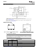
CONNECTION DIAGRAMS
Top View Top View
Figure 1. SOT-23, 5-Lead Small Outline Package Figure 2. DSBGA Package, 5-Bump Package
(M5)
See Package Numbers YPB0005 and YZR0005
See Package Number DBV0005A
NOTE
The actual physical placement of the package marking will vary from part to part. Package
marking contains date code and lot traceability information, and will vary considerably.
Package marking does not correlate to device type.
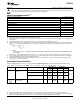
PIN DESCRIPTIONS
Pin Number
Name Function
SOT-23 DSBGA
V
IN
1 C3 Input Voltage
GND 2 A1 Common Ground (device substrate)
ON/OFF 3 A3 Logic high enable input
BYPASS 4 B2 Bypass capacitor for low noise operation
V
OUT
5 C1 Regulated output voltage
2 Submit Documentation Feedback Copyright © 2000–2013, Texas Instruments Incorporated
Product Folder Links: LP2985-N