SIM7100 Series Hardware Design V1.
Smart Machine Smart Decision Document Title SIM7100 Series Hardware Design Version 1.02 Date 2015-06-16 Status Released Document Control ID SIM7100_Series_Hardware_Design_V1.02 General Notes SIMCom offers this information as a service to its customers to support the application and engineering efforts that use the products designed by SIMCom. The information provided is based on the requirements specifically from the customers.
Smart Machine Smart Decision Contents General Notes .................................................................................................................................... 2 Copyright ........................................................................................................................................... 2 Contents ............................................................................................................................................. 3 Table Index .......
Smart Machine Smart Decision 3.8.1 I2C Design Guide ......................................................................................................... 38 3.9 Keypad Interface ................................................................................................................. 39 3.9.1 Keypad Application Guide ........................................................................................... 39 3.10 SPI Interface ...................................................................
Smart Machine Smart Decision Table Index Table 1: SIM7100 series frequency bands...................................................................................................... 8 Table 2: General Features ............................................................................................................................ 11 Table 3: Pin Definition.................................................................................................................................
Smart Machine Smart Decision Figure Index Figure 1: SIM7100 Block Diagram ..............................................................................................................10 Figure 2: Pin Assignment Overview .............................................................................................................13 Figure 3: Top dimensions (Unit: mm) ...........................................................................................................
Smart Machine Smart Decision Revision History Data Version Description of change Author 2015-01-20 1.01 Original Yang Hongliang Li Ya 2015-06-16 1.02 Add the description of SIM7100CT. Add the label description. Yang Hongliang Li Ya SIM7100_Hardware_Design_V1.
Smart Machine Smart Decision 1 Introduction This document describes the electronic specifications, RF specifications, interfaces, mechanical characteristics and testing results of the SIMCom SIM7100 series modules. With the help of this document and other SIM7100 software application notes/user guides, users can understand and use SIM7100 series modules to design and develop applications quickly. 1.
Smart Machine Smart Decision LTE-FDD B18 P LTE-FDD B19 P P LTE-FDD B20 LTE TDD B38 P P P LTE TDD B39 P P P LTE TDD B40 P P P LTE TDD B41 P P P GPS P P P P P P P GLONASS P P P P P P P LTE-TDD GNSS P P P With a tiny physical dimension of 30*30*2.9 mm and the functions integrated, the SIM7100 series modules can meet almost any space requirement in users’ applications, such as smart phone, PDA, industrial handheld, machine-to-machine and vehicle application, etc.
Smart Machine Smart Decision 1.3 Hardware Block Diagram The block diagram of the SIM7100 is shown in the figure below. Figure 1: SIM7100 Block Diagram SIM7100_Hardware_Design_V1.
Smart Machine Smart Decision 1.4 Functional Overview Table 2: General Features Feature Implementation Power supply Single supply voltage 3.4~4.2V Power saving l Radio frequency bands Please refer to the table 1 GSM/GPRS: l Class 4 (2W): GSM850、EGSM900 l Class 1 (1W): DCS1800、PCS1900 EDGE: l Class E2 (0.5W): GSM850、EGSM900 l Class E1 (0.4W): DCS1800、PCS1900 UMTS: l Class 3 (0.25W): WCDMA l Class 3 (0.25W): CDMA2000 l Class 2 (0.25W): TD-SCDMA LTE: l Class 3 (0.
Smart Machine Smart Decision l l Support PCM interface Only support PCM master mode and short frame sync, 16-bit linear data formats l l l l l l A full modem serial port by default Baud rate: 300bps to 4Mbps(default:115200bps) Autobauding baud rate: 1200 bps to 115200bps Can be used as the AT commands or data stream channel. Support RTS/CTS hardware handshake and software ON/OFF flow control Multiplex ability according to GSM 07.10 Multiplexer Protocol.
Smart Machine Smart Decision 2 Package Information 2.1 Pin Assignment Overview All functions of the SIM7100 will be provided through 87 pads that will be connected to the customers’ platform. The following Figure is a high-level view of the pin assignment of the SIM7100.
Smart Machine Smart Decision Table 3: Pin Definition Pad No. Pad Name Pad No.
Smart Machine Smart Decision 69 RI 70 DCD 71 TXD 72 DTR 73 PCM_OUT 74 PCM_IN 75 PCM_SYNC 76 PCM_CLK 77 GND 78 GND 79 GNSS_ANT 80 GND 81 GND 82 MAIN_ANT 83 COEX1 84 COEX2 85 BOOT_CFG0 86 COEX3 87 BOOT_CFG1 2.
Smart Machine Smart Decision VDD_EXT 44 PO LDO power output for SD card circuit or other external circuit with Max. 150mA current output. Its output voltage is Configurable(The If unused, keep it open. default voltage is 0V). VDD_1V8 15 GND 1,2, 5, 10, 14, 37, 40, 41, 43, 57, 58, 60, 61, 64, 65, 77, 78, 80, 81 PO 1.8V SMPS output with Max. 50mA current output for external circuit, such as level shift circuit. If unused, keep it open.
Smart Machine Smart Decision USIM_DATA 17 I/O,PU USIM Card data I/O, which has been pulled up via a 20KR resistor to USIM_VDD internally. Do not pull it up or down externally. USIM_RST 18 DO USIM Reset USIM_CLK 19 DO USIM clock 20 PO Power output for USIM card, its output Voltage depends on USIM card type automatically. Its output current is up to 50mA.
Smart Machine Smart Decision Keypad interface KBR0 29 DOH Bit 0 drive to the pad matrix KBR1 33 DOH Bit 1 drive to the pad matrix KBR2 30 DOH Bit 2 drive to the pad matrix KBR3 35 DOH Bit 3 drive to the pad matrix KBR4 34 DOH Bit 4 drive to the pad matrix DI,PD Bit 0 for sensing key press on pad matrix KBC0 28 KBC1 27 KBC2 31 KBC3 32 KBC4 36 DI,PD Bit 1 for sensing key press on pad matrix DI,PD Bit 2 for sensing key press on pad matrix DI,PD Bit 3 for sensing key press
Smart Machine Smart Decision AUX_ANT 59 AI Auxiliary antenna soldering pad ISINK 45 PO Ground-referenced current sink. ADC1 47 AI Analog-digital converter input 1 ADC2 46 AI Analog-digital converter input 2 COEX1 83 I/O COEX2 84 I/O COEX3 86 I/O Other interface BOOT_CFG0 85 DI,PD BOOT_CFG1 87 DI,PD If unused, please keep them open. RF synchronizing between Wi-Fi and LTE. If unused, keep them open. Boot configuration input.
Smart Machine Smart Decision 2.3 Mechanical Information The following figure shows the package outline drawing of SIM7100. Figure 3: Top dimensions (Unit: mm) SIM7100_Hardware_Design_V1.
Smart Machine Smart Decision Figure 4: Side dimensions (Unit: mm) SIM7100_Hardware_Design_V1.
Smart Machine Smart Decision Figure 5: Bottom dimensions (Unit: mm) SIM7100_Hardware_Design_V1.
Smart Machine Smart Decision 2.4 Footprint Recommendation Figure 6: Footprint Recommendation (Unit: mm) SIM7100_Hardware_Design_V1.
Smart Machine Smart Decision 3 Interface Application 3.1 Power Supply The power supply pins of SIM7100 include 4 pins (pin 62&63, pin 38&39) named VBAT. The 4 VBAT pads supplies the power to RF and baseband circuits directly. On VBAT pads, the ripple current up to 2A typically, due to GSM/GPRS emission burst (every 4.615ms), may cause voltage drop. So the power supply for these pads must be able to provide sufficient current up to more than 2A in order to avoid the voltage drop is more than 300mV.
Smart Machine Smart Decision 3.1.1 Power supply Design Guide Make sure that the voltage on the VBAT pins will never drop below 3.4V even during a transmit burst, when current consumption may rise up to 2A. If the voltage drops below 3.4V, the RF performance may be affected.
Smart Machine Smart Decision 3.1.2 Recommended Power supply circuit GND It is recommended that a switching mode power supply or linear regulator power supply is used. It is important to make sure that all the components used in the power supply circuit can resist a peak current up to 2A. The following figure shows the linear regulator reference circuit with 5V input and 3.8V output.
Smart Machine Smart Decision 3.2 3.2.1 Power on/Power off/Reset Function Power on SIM7100 can be powered on by pulling the PWRKEY pin down to ground. The PWRKEY pin has been pulled up with a 200KΩ resistor to 1.8V internally, so it does not need to pull it up externally. It is strongly recommended to put a100nF capacitor and an ESD protection diode close to the PWRKEY pin. Please refer to the following figure for the recommended reference circuit.
Smart Machine Smart Decision Table 8: Power on timing and Electronic Characteristic Symbol Parameter Min. Typ. Max. Ton The time of active low level impulse of PWRKEY pin to power on module Ton(status) 100 500 - The time from power-on issue to STATUS pin output high level(indicating power up ready ) 15 - 25 Ton(uart) The time from power-on issue to UART port ready 10 - 20 VIH Input high level voltage on PWRKEY pin 1.17 1.8 2.1 V VIL Input low level voltage on PWRKEY pin -0.
Smart Machine Smart Decision Table 9: Power off timing and Electronic Characteristic Symbol Parameter Time value Min. Typ. Max. Unit Toff The active low level time pulse on PWRKEY pin to power off module 2.
Smart Machine Smart Decision Table 10: RESET Pin Electronic Characteristic Symbol Description Min. Typ. Max. Unit Treset The active low level time impulse on RESET pin to reset module 50 100 500 ms VIH Input high level voltage 1.17 1.8 2.1 V VIL Input low level voltage -0.3 0 0.3 V 3.3 UART Interface SIM7100 provides a 7-wire UART (universal asynchronous serial transmission) interface as DCE (Data Communication Equipment).
Smart Machine Smart Decision interface, the level shifter circuits should be used for voltage matching. The TXB0108RGYR provided by Texas Instruments is recommended. The following figure shows the voltage matching reference design. Figure 17: Reference circuit of level shift To comply with RS-232-C protocol, the RS-232-C level shifter chip should be used to connect SIM7100 to the RS-232-C interface, for example SP3238ECA, etc.
Smart Machine Smart Decision until the call is answered or hung up. Figure 19: RI behaviour(voice call) Note: For more details of AT commands about UART, please refer to document [1] and [22]. DTR pin can be used to wake SIM7100 from sleep. When SIM7100 enters sleep mode, pulling down DTR can wake SIM7100. 3.4 USB Interface The SIM7100 contains a USB interface compliant with the USB2.0 specification as a peripheral, but the USB charging function is not supported. 3.4.
Smart Machine Smart Decision 3.5 USIM Interface SIM7100 supports both 1.8V and 3.0V USIM Cards. Table 11: USIM Electronic characteristic in 1.8V mode (USIM_VDD =1.8V) Symbol Parameter Min. Typ. Max. Unit USIM_VDD LDO power output voltage 1.75 1.8 1.95 V VIH High-level input voltage 0.65·USIM_VDD - USIM_VDD +0.3 V VIL Low-level input voltage -0.3 0 0.35·USIM_VDD V VOH High-level output voltage - USIM_VDD V VOL Low-level output voltage 0 0.45 V USIM_VDD -0.
Smart Machine Smart Decision Figure 21: USIM interface reference circuit Note: USIM_DATA has been pulled up with a 20KΩ resistor to USIM_VDD in module. A 220nF capacitor on USIM_VDD is used to reduce interference. For more details of AT commands about USIM, please refer to document [1]. 3.5.2 Recommended USIM Card Holder It is recommended to use the 6-pin USIM socket such as C707 10M006 512 produced by Amphenol. User can visit http://www.amphenol.com for more information about the holder.
Smart Machine Smart Decision Table 13: Amphenol USIM Socket Pin Description Pin C1 C2 Signal USIM_VDD USIM_RST Description USIM Card Power supply. USIM Card Reset. C3 C5 C6 C7 USIM_CLK GND VPP USIM_DATA USIM Card Clock. Connect to GND. 3.6 USIM Card data I/O. PCM Interface SIM7100 provides a PCM interface for external codec, which can be used in master mode with short sync and 16 bits linear format.
Smart Machine Smart Decision Figure 24: EXT CODEC to MODULE timing Figure 25: MODULE to EXT CODEC timing Table 15: PCM Timing parameters Parameter Description Min. Typ. Max. Unit T(sync) PCM_SYNC cycle time – 125 – μs T(synch) PCM_SYNC high level time – 488 – ns T(syncl) PCM_SYNC low level time – 124.
Smart Machine Smart Decision 3.6.2 PCM Application Guide The following figure shows the external codec reference design. Figure 26: Audio Codec Reference Circuit Note: SIM7100 can transmit PCM data by the USB port besides the PCM interface. For more details please refer to documents [1] and [23]. 3.7 SD Interface SIM7100 provides a 4-bit SD/MMC interface with clock rate up to 52 MHz. The voltage of MMC/SD interface is 2.
Smart Machine Smart Decision **VDD_EXT must be set with 2.95V output by AT command. 3.7.1 SD Design guide 4.7uF 100nF TVS 33pF TVS 33pF TVS 33pF TVS 33pF TVS 33pF TVS 33pF VDD_EXT can provide power for SD card. ESD/EMI components should be arranged beside SD card socket. Refer to the following application circuit. Figure 27: SD Reference Circuit Note: The SD signal lines have internal pull-up resistors for BOM saving. 3.
Smart Machine Smart Decision needed in application circuit. “AT+CRIIC and AT+CWIIC” AT commands could be used to read/write register values of the I2C peripheral devices. For more details about AT commands please refer to document [1]. 3.9 Keypad Interface SIM7100 provides a keypad interface, which supports five sense columns, and five keypad rows. The interface will generate a interrupt when any key is pressed. Its operation voltage is 1.8V. 3.9.
Smart Machine Smart Decision Figure 30: NETLIGHT Reference Circuit Note: The value of the resistor named “R” depends on the LED characteristic. Table 17: NETLIGHT Pin Status NETLIGHT Pin Status Always On 200ms ON, 200ms OFF 800ms ON, 800ms OFF Module Status Searching Network/Call Connect Data Transmit Registered network OFF Power off / Sleep Note: NETLIGHT output low level as “OFF”, and high level as “ON”. 3.
Smart Machine Smart Decision Table 18: FLIGHTMODE Pin Status FLIGHTMODE Pin Status Input Low Level Input High Level Module operation Flight Mode: RF is closed. Normal Mode: RF is working. 3.13 Pin multiplex Function Some pins of SIM7100 could be used for alternate function besides default function.
Smart Machine Smart Decision 3.13.1 SD2 Interface The Keypad pins can be multiplexed with SD2 pins. The SD2 is a SDIO 2.0 interface compatible with WLAN (802.11), its operation voltage is 1.8V. Table 20: SD2 Pin description Pin name Pin No. Function KBR2 30 SD2_DATA0 KBC1 27 SD2_DATA1 KBC0 28 SD2_DATA2 KBC2 31 SD2_DATA3 KBR0 29 SD2_CMD KBC3 32 SD2_CLK Note: SD2 function is only used in Wi-Fi solution. For more details, please contact SIMCom. 3.14 Other interface 3.14.
Smart Machine Smart Decision Figure 32: ISINK Reference Circuit Note: The sinking current can be adjusted to meet the design requirement through the AT command “AT+ CLEDITST =<0>, ”.The “value” ranges from 0 to 8, on behalf of the current from 0mA to 40mA by 5mA step. 3.14.2 ADC SIM7100 has 2 dedicated ADC pins named ADC1 and ADC2.They are available for digitizing analog signals such as battery voltage and so on. These electronic specifications are shown in the following table.
Smart Machine Smart Decision 3.14.3 LDO SIM7100 has a LDO power output, named VDD_EXT. its output voltage is 0V by default, Users can switch the LDO on or off by the AT command “AT+CVAUXS” and configure its output voltage by the AT command “AT+CVAUXV”. Table 23: Electronic characteristic Symbol Description Min. Typ. Max. Unit VVDD_EXT Output voltage 1.7 2.95 3.05 V IO Output current - - 150 mA Note:For more details of AT commands about VDD_EXT, please refer to document [1].
Smart Machine Smart Decision 4 RF Specifications 4.
Smart Machine Smart Decision WCDMA B6 WCDMA B8 875~885 MHz 830~840 MHz 925~960 MHz 880~915 MHz TDSCDMA 1.9G TDSCDMA 2G 1880~1920 MHz 2010~2025 MHz 1880~1920 MHz 2010~2025 MHz CDMA BC0 869~894 824~849 MHz MHz The LTE Operating frequencies are shown in the following table 26. Note: Operating frequencies of LTE TDD B41 for the SIM7100C is 100MHz BW, 2555~2655 MHz GPS L1 BAND 1574.4 ~1576.
Smart Machine Smart Decision 31 452.5 MHz~457.5 MHz 462.5 MHz~467.
Smart Machine Smart Decision 9 - - -99 -96 -94.2 -93 FDD 10 - - -100 -97 -95.2 -94 FDD 11 - - -100 -97 FDD 12 -101.7 -98.7 -97 -94 FDD -97 -94 FDD - -97 -94 FDD FDD 13 14 17 - - -97 -94 18 - - -100 -97 -95.2 - FDD 19 - - -100 -97 -95.2 - FDD 20 -97 -94 -91.2 -90 FDD 21 -100 -97 -95.2 22 -97 -94 -92.2 -100 -97 FDD -100 -97 FDD 23 -104.7 -101.7 24 FDD -91 FDD 25 -101.2 -98.2 -96.5 -93.5 -91.7 -90.
Smart Machine Smart Decision 4.2 GSM/UMTS/LTE Antenna Design Guide Users should connect antennas to SIM7100’s antenna pads through micro-strip line or other types of RF trace and the trace impedance must be controlled in 50Ω. SIMCom recommends that the total insertion loss between the antenna pads and antennas should meet the following requirements: ● GSM900/GSM850<0.5dB ● DCS1800/PCS1900 <0.9dB ● WCDMA 2100/1900<0.9dB ● WCDMA 900/850<0.5 dB ● TDSCDMA 1900/2100<0.5dB ● CDMA BC0<0.5dB ● LTE (F<1GHz) <0.
Smart Machine Smart Decision Figure 34: Antenna matching circuit (AUX_ANT) In above figure, R3, C3, C4 and R4 are used for auxiliary antenna matching. By default, the R3, R4 are 0Ωresistors, and the C3, C4 are reserved for tuning. Note:SIMCom suggests the LTE auxiliary antenna to be kept on, since there are many high bands in the designing of TDD-LTE, such as band38, band40 and band41.
Smart Machine Smart Decision Note: If the antenna is active type, the power should be given by main board, because there is no power supply on GPS antenna pad. If the antenna is passive, it is suggested that the external LNA should be used. 4.3.2 GNSS Application Guide Users can adopt an active antenna or a passive antenna as GNSS signal transceiver. In this document, all GNSS specification mentioned is from passive antenna. The following is the reference circuit.
Smart Machine Smart Decision antenna characteristic, and VDD can be shut down to avoid consuming additional current when not being used. GNSS can be used by NMEA port. User can select NMEA as output through UART or USB. NMEA sentences are automatic and no command is provided. NMEA sentences include GSV, GGA, RMC, GSA, and VTG. Before using GNSS, user should configure SIM7100 in proper operating mode by AT command. Please refer to related document for details.
Smart Machine Smart Decision 5 Electrical Specifications 5.1 Absolute maximum ratings Absolute maximum rating for digital and analog pins of SIM7100 are listed in the following table: Table 29: Absolute maximum ratings Parameter Voltage at VBAT Voltage at USB_VBUS Voltage at digital pins (PWRKEY,RESET,SPI,Keypad,GPIO,I2C,UART,PCM) Voltage at digital pins (SD,USIM) 5.2 Min. -0.5 -0.5 Max. 6.0 5.25 Unit V V -0.3 2.1 V -0.3 3.05 V Typ. 3.8 5 Max. 4.2 5.25 Unit V V Typ. Max.
Smart Machine Smart Decision FLIGHTMODE, STATUS, USIM_DET, SD1_DET), I2C, UART, PCM, COEXn, and BOOT_CFGn. The operating temperature of SIM7100 is listed in the following table. Table 32: Operating temperature Parameter Normal operation temperature Min. -30 Typ. 25 Max. 80 Unit ℃ Extended operation temperature* -40 25 85 ℃ Storage temperature -45 25 +90 ℃ *Note: Module is able to make and receive voice calls, data calls, SMS and make GPRS/WCDMA/HSPA+/LTE traffic in -40℃ ~ +85℃.
Smart Machine Smart Decision accessible. The power consumption in this mode is lower than normal mode. Flight mode AT command “AT+CFUN=4” or pulling down the FLIGHTMODE pin can be used to set the module to flight mode without removing the power supply. In this mode, the RF part of the module will not work, but the serial port and USB port are still accessible. The power consumption in this mode is lower than normal mode.
Smart Machine Smart Decision 5.4 Current Consumption The current consumption is listed in the table below. Table 34: Current consumption on VBAT Pins (VBAT=3.8V) GNSS GNSS supply current (AT+CFUN=0,with USB connection) @ -140dBm,Tracking Typical:72mA GSM Sleep mode/Idle Mode GSM/GPRS supply current (GNSS off,without USB connection) Sleep mode@ BS_PA_MFRMS=2 Typical: 4.
Smart Machine Smart Decision ( 1 Rx,4 Tx ) DCS1800 ( 1 Rx,4 Tx ) GSM 900 ( 3Rx, 2 Tx ) DCS1800 ( 3Rx, 2 Tx ) HSDPA Data WCDMA B1 WCDMA B2 WCDMA B5 WCDMA B6 WCDMA B8 TD-SCDMA Data TDSCDMA 1900 TDSCDMA 2000 EVDO Data BC0 LTE Data LTE-FDD B1 LTE-FDD B2 LTE-FDD B3 LTE-FDD B4 LTE-FDD B5 LTE-FDD B7 LTE-FDD B8 LTE-FDD B13 LTE-FDD B17 LTE-FDD B18 LTE-FDD B20 LTE-TDD B38 LTE-TDD B39 LTE-TDD B40 SIM7100_Hardware_Design_V1.
Smart Machine Smart Decision LTE-TDD B41 5.5 @10Mbps Typical: 416mA @15Mbps Typical: 445mA @5Mbps Typical: 417mA @10Mbps Typical: 428mA @15Mbps Typical: 448mA ESD Notes SIM7100 is sensitive to ESD in the process of storage, transporting and assembling. Especially, SIM7100 is mounted on the users’ mother board, The ESD components should be placed beside the connectors which human body might touch, such as USIM card holder, audio jacks, switches and keys, etc.
Smart Machine Smart Decision 6 SMT Production Guide 6.1 Top and Bottom View of SIM7100 Figure 37: Top and bottom view of SIM7100 Note: The 10 circular test points on bottom are only used for testing. They cannot be used for users’ application circuit. SIM7100_Hardware_Design_V1.
Smart Machine Smart Decision 6.2 Label Information Figure 38: Label Information Table 36: The Description of Label Information No. Description A LOGO B No.1 Pin C Project Name D Product Code E Serial Number F International Mobile Equipment Identity G QR code SIM7100_Hardware_Design_V1.
Smart Machine Smart Decision 6.3 Typical SMT Reflow Profile SIMCom provides a typical soldering profile. Therefore the soldering profile shown below is only a generic recommendation and should be adjusted to the specific application and manufacturing constraints. Figure 39: The ramp-soak-spike Reflow Profile of SIM7100 Note: For more details about secondary SMT, please refer to the document [21]. 6.
Smart Machine Smart Decision time limit specified on the label. NOTE: IPC / JEDEC J-STD-033 standard must be followed for production and storage. 6.5 Stencil Foil Design Recommendation The recommended thickness of stencil foil is more than 0.15mm. SIM7100_Hardware_Design_V1.
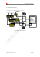
Smart Machine Smart Decision Appendix A. Reference Design Main Antenna GNSS Antenna R102 0R 82 NC C106 NC C107 C101 100uF C102 100uF C103 1uF 79 GND 77 58 GND GND 78 62 VBAT GNSS_ANT GND 60 Power supply MAIN_ANT 57 GND VBAT 63 61 GND 64 GND GND 80 AUX_ANT 59 GND 41 L101 NC C108 33pF L102 NC R101 VBAT Div Antenna 0R C104 NC C105 NC R105 3 POWERKEY 300R NETLIGHT R103 4.
Smart Machine Smart Decision B. Coding Schemes and Maximum Net Data Rates over Air Interface Table 38: Coding Schemes and Maximum Net Data Rates over Air Interface Multislot definition(GPRS/EDGE) Slot class DL slot number UL slot number Active slot number 1 2 3 4 5 6 7 8 9 10 11 12 1 2 2 3 2 3 3 4 3 4 4 4 1 1 2 1 2 2 3 1 2 2 3 4 2 3 3 4 4 4 4 5 5 5 5 5 GPRS coding scheme Max data rata(4 slots) Modulation type CS 1 = 9.05 kb/s / time slot 36.2 kb/s GMSK CS 2 = 13.4 kb/s / time slot 53.
Smart Machine Smart Decision Category 8 7.2Mbps 16QAM,QPSK Category 9 10.2Mbps 16QAM,QPSK Category 10 14.4Mbps 16QAM,QPSK Category 11 0.9Mbps QPSK Category 12 1.8Mbps QPSK Category 13 17.6Mbps 64QAM Category 14 21.1Mbps 64QAM Category 15 23.4Mbps 16QAM Category 16 28Mbps 16QAM Category 17 23.4Mbps 64QAM Category 18 28Mbps 64QAM Category 19 35.5Mbps 64QAM Category 20 42Mbps 64QAM Category 21 23.4Mbps 16QAM Category 22 28Mbps 16QAM Category 23 35.
Smart Machine Smart Decision C. Related Documents Table 39: Related documents SN [1] [2] Title SIM7100_ATC_V0.xx ITU-T Draft new recommendationV.25ter [3] GSM 07.07 [4] GSM 07.10 [5] GSM 07.05 [6] GSM 11.14 [7] GSM 11.11 [8] GSM 03.38 [9] GSM 11.10 [10] 3GPP TS 51.010-1 [11] 3GPP TS 34.124 [12] 3GPP TS 34.121 [13] 3GPP TS 34.123-1 [14] 3GPP TS 34.123-3 [15] EN 301 908-02 V2.2.1 [16] EN 301 489-24 V1.2.1 SIM7100_Hardware_Design_V1.02 Description SIM7100_ATC_V0.
Smart Machine Smart Decision [17] IEC/EN60950-1(2001) Safety of information technology equipment (2000) [18] 3GPP TS 51.010-1 Digital cellular telecommunications system (Release 5); Mobile Station (MS) conformance specification [19] GCF-CC V3.23.
Smart Machine Smart Decision D.
Smart Machine Smart Decision SIM SMS SPI SMPS TDMA TE TX UART VSWR SM NC EDGE HSDPA HSUPA ZIF WCDMA VCTCXO USIM UMTS UART Subscriber Identification Module Short Message Service serial peripheral interface Switched-mode power supply Time Division Multiple Access Terminal Equipment, also referred to as DTE Transmit Direction Universal Asynchronous Receiver & Transmitter Voltage Standing Wave Ratio SIM phonebook Not connect Enhanced data rates for GSM evolution High Speed Downlink Packet Access High Speed Up
Smart Machine Smart Decision E. Safety Caution Table 41: Safety caution Marks Requirements When in a hospital or other health care facility, observe the restrictions about the use of mobiles. Switch the cellular terminal or mobile off, medical equipment may be sensitive to not operate normally for RF energy interference. Switch off the cellular terminal or mobile before boarding an aircraft. Make sure it is switched off.
Smart Machine Smart Decision Contact us: Shanghai SIMCom Wireless Solutions Ltd. Add: SIM Technology Building, No.633, Jinzhong Road, Changning District, Shanghai P.R. China 200335 Tel: +86 21 3235 3300 Fax: +86 21 3235 3301 URL: www.sim.com/wm SIM7100_Hardware_Design_V1.