
Data Sheet
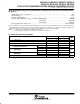


SN54LS373, SN54LS374, SN54S373, SN54S374,
SN74LS373, SN74LS374, SN74S373, SN74S374
OCTAL D-TYPE TRANSPARENT LATCHES AND EDGE-TRIGGERED FLIP-FLOPS
SDLS165B – OCTOBER 1975 – REVISED AUGUST 2002
1
POST OFFICE BOX 655303 • DALLAS, TEXAS 75265
Choice of Eight Latches or Eight D-Type
Flip-Flops in a Single Package
3-State Bus-Driving Outputs
Full Parallel Access for Loading
Buffered Control Inputs
Clock-Enable Input Has Hysteresis to
Improve Noise Rejection (’S373 and ’S374)
P-N-P Inputs Reduce DC Loading on Data
Lines (’S373 and ’S374)
description
These 8-bit registers feature 3-state outputs
designed specifically for driving highly capacitive
or relatively low-impedance loads. The
high-impedance 3-state and increased
high-logic-level drive provide these registers with
the capability of being connected directly to and
driving the bus lines in a bus-organized system
without need for interface or pullup components.
These devices are particularly attractive for
implementing buffer registers, I/O ports,
bidirectional bus drivers, and working registers.
The eight latches of the ’LS373 and ’S373 are
transparent D-type latches, meaning that while
the enable (C or CLK) input is high, the Q outputs
follow the data (D) inputs. When C or CLK is taken
low, the output is latched at the level of the data
that was set up.
The eight flip-flops of the ’LS374 and ’S374 are
edge-triggered D-type flip-flops. On the positive
transition of the clock, the Q outputs are set to the
logic states that were set up at the D inputs.
Schmitt-trigger buffered inputs at the enable/clock lines of the ’S373 and ’S374 devices simplify system design
as ac and dc noise rejection is improved by typically 400 mV due to the input hysteresis. A buffered
output-control (OC
) input can be used to place the eight outputs in either a normal logic state (high or low logic
levels) or the high-impedance state. In the high-impedance state, the outputs neither load nor drive the bus lines
significantly.
OC
does not affect the internal operation of the latches or flip-flops. That is, the old data can be retained or new
data can be entered, even while the outputs are off.
Copyright 2002, Texas Instruments Incorporated
Please be aware that an important notice concerning availability, standard warranty, and use in critical applications of
Texas Instruments semiconductor products and disclaimers thereto appears at the end of this data sheet.
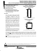
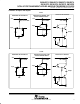
SN54LS373, SN54LS374, SN54S373,
SN54S374 . . . J OR W PACKAGE
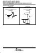
SN74LS373, SN74S374 . . . DW, N, OR NS PACKAGE
SN74LS374 . . . DB, DW, N, OR NS PACKAGE
SN74S373 . . . DW OR N PACKAGE
(TOP VIEW)
3212019
910111213
4
5
6
7
8
18
17
16
15
14
8D
7D
7Q
6Q
6D
2D
2Q
3Q
3D
4D
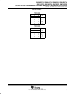
SN54LS373, SN54LS374, SN54S373,
SN54S374 . . . FK PACKAGE
(TOP VIEW)
1D
1Q
OC
5Q
5D
8Q
4Q
GND
C
V
CC
1
2
3
4
5
6
7
8
9
10
20
19
18
17
16
15
14
13
12
11
OC
1Q
1D
2D
2Q
3Q
3D
4D
4Q
GND
V
CC
8Q
8D
7D
7Q
6Q
6D
5D
5Q
C
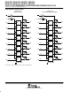
†
†
C for ’LS373 and ’S373; CLK for ’LS374 and ’S374.
†
C for ’LS373 and ’S373; CLK for ’LS374 and ’S374.
†
PRODUCTION DATA information is current as of publication date.
Products conform to specifications per the terms of Texas Instruments
standard warranty. Production processing does not necessarily include
testing of all parameters.
On products compliant to MIL-PRF-38535, all parameters are tested
unless otherwise noted. On all other products, production
processing does not necessarily include testing of all parameters.