
Data Sheet


www.ti.com
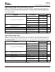
ELECTRICAL CHARACTERISTICS
TAS5142
SLES126B – DECEMBER 2004 – REVISED MAY 2005
R
L
= 4 Ω , F
PWM
= 384 kHz, unless otherwise noted. All performance is in accordance with recommended operating conditions
unless otherwise specified.
TAS5142
PARAMETER TEST CONDITIONS UNIT
MIN TYP MAX
Internal Voltage Regulator and Current Consumption
Voltage regulator, only used as a
VREG VDD = 12 V 3 3.3 3.6 V
reference node
Operating, 50% duty cycle 7 17
IVDD VDD supply current mA
Idle, reset mode 6 11
50% duty cycle 5 16
IGVDD_X Gate supply current per half-bridge mA
Reset mode 0.3 1
50% duty cycle, without output filter or load 15 25 mA
IPVDD_X Half-bridge idle current
Reset mode, no switching 7 25 µ A
Output Stage MOSFETs
T
J
= 25°C, includes metallization resistance,
R
DSon,LS
Drain-to-source resistance, LS 140 155 m Ω
GVDD = 12 V
T
J
= 25°C, includes metallization resistance,
R
DSon,HS
Drain-to-source resistance, HS 140 155 m Ω
GVDD = 12 V
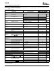
I/O Protection
Undervoltage protection limit,
V
uvp,G
9.8 V
GVDD_X
V
uvp,hyst
(1)
250 mV
OTW
(1)
Overtemperature warning 115 125 135 °C
Temperature drop needed below
OTW
HYST
(1)
OTW temp. for OTW to be inactive 25 °C
after the OTW event
OTE
(1)
Overtemperature error 145 155 165 °C
OTE-
OTE-OTW differential 30 °C
OTW
differential
(1)
A reset event must occur for SD to
OTE
HYST
(1)
25 °C
be released following an OTE event.
OLPC Overload protection counter F
PWM
= 384 kHz 1.25 ms
Resistor—programmable, high-end,
I
OC
Overcurrent limit protection 7.9 9.7 11.4 A
R
OCP
= 18 k Ω
I
OCT
Overcurrent response time 210 ns
R
OCP
OC programming resistor range Resistor tolerance = 5% 18 69 k Ω
Connected when RESET is active to provide
Internal pulldown resistor at the
R
PD
bootstrap capacitor charge. Not used in SE 2.5 k Ω
output of each half-bridge
mode
Static Digital Specifications
V
IH
High-level input voltage 2 V
PWM_A, PWM_B, PWM_C, PWM_D, M1,
M2, M3, RESET_AB, RESET_CD
V
IL
Low-level input voltage 0.8 V
Leakage Input leakage current –10 10 µ A
OTW/SHUTDOWN (SD)
Internal pullup resistance, OTW to
R
INT_PU
20 26 32 k Ω
VREG, SD to VREG
Internal pullup resistor 3 3.3 3.6
V
OH
High-level output voltage V
External pullup of 4.7 k Ω to 5 V 4.5 5
V
OL
Low-level output voltage I
O
= 4 mA 0.2 0.4 V
FANOUT Device fanout OTW, SD No external pullup 30 Devices
(1) Specified by design
10