
Data Sheet


www.ti.com
GENERAL INFORMATION
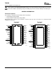
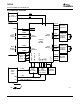
Terminal Assignment
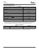
1
2
3
4
5
6
7
8
9
10
11
12
13
14
15
16
17
18
36
35
34
33
32
31
30
29
28
27
26
25
24
23
22
21
20
19
GVDD_B
OTW
SD
PWM_A
RESET_AB
PWM_B
OC_ADJ
GND
AGND
VREG
M3
M2
M1
PWM_C
RESET_CD
PWM_D
VDD
GVDD_C
GVDD_A
BST_A
PVDD_A
OUT_A
GND_A
GND_B
OUT_B
PVDD_B
BST_B
BST_C
PVDD_C
OUT_C
GND_C
GND_D
OUT_D
PVDD_D
BST_D
GVDD_D
DKD PACKAGE
(TOP VIEW)
P0018-01
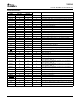
1
2
3
4
5
6
7
8
9
10
11
12
13
14
15
16
17
18
19
20
21
22
GVDD_B
OTW
NC
NC
SD
PWM_A
RESET_AB
PWM_B
OC_ADJ
GND
AGND
VREG
M3
M2
M1
PWM_C
RESET_CD
PWM_D
NC
NC
VDD
GVDD_C
DDV PACKAGE
(TOP VIEW)
GVDD_A
BST_A
NC
PVDD_A
PVDD_A
OUT_A
GND_A
GND_B
OUT_B
PVDD_B
BST_B
BST_C
PVDD_C
OUT_C
GND_C
GND_D
OUT_D
PVDD_D
PVDD_D
NC
BST_D
GVDD_D
44
43
42
41
40
39
38
37
36
35
34
33
32
31
30
29
28
27
26
25
24
23
P0016-02
TAS5142
SLES126B – DECEMBER 2004 – REVISED MAY 2005
These devices have limited built-in ESD protection. The leads should be shorted together or the device
placed in conductive foam during storage or handling to prevent electrostatic damage to the MOS gates.
The TAS5142 is available in two thermally enhanced packages:
• 36-pin PSOP3 package (DKD)
• 44-pin HTSSOP PowerPad™ package (DDV)
Both package types contain a heat slug that is located on the top side of the device for convenient thermal
coupling to the heatsink.
2