
Data Sheet


www.ti.com
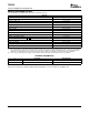
MODE Selection Pins for Both Packages
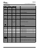
Package Heat Dissipation Ratings
(1)
TAS5142
SLES126B – DECEMBER 2004 – REVISED MAY 2005
GENERAL INFORMATION (continued)
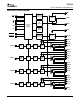
MODE PINS
PWM INPUT OUTPUT CONFIGURATION PROTECTION SCHEME
M3 M2 M1
0 0 0 2N
(1)
AD/BD modulation 2 channels BTL output BTL mode
(2)
0 0 1 Reserved
0 1 0 1N
(1)
AD modulation 2 channels BTL output BTL mode
(2)
0 1 1 1N
(1)
AD modulation 1 channel PBTL output PBTL mode. Only PWM_A input is used.
Protection works similarly to BTL mode
(2)
. Only
difference in SE mode is that OUT_X is Hi-Z
1 0 0 1N
(1)
AD modulation 4 channels SE output
instead of a pulldown through internal pulldown
resistor.
1 0 1
1 1 0 Reserved
1 1 1
(1) The 1N and 2N naming convention is used to indicate the required number of PWM lines to the power stage per channel in a specific
mode.
(2) An overload protection (OLP) occurring on A or B causes both channels to shut down. An OLP on C or D works similarly. Global errors
like overtemperature error (OTE), undervoltage protection (UVP), and power-on reset (POR) affect all channels.
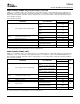
PARAMETER TAS5142DKD TAS5142DDV
R
θ JC
(°C/W)—2 BTL or 4 SE channels (8 transistors) 1.28 1.28
R
θ JC
(°C/W)—1 BTL or 2 SE channel(s) (4 transistors) 2.56 2.56
R
θ JC
(°C/W)—(1 transistor) 8.6 8.6
Pad area
(2)
80 mm
2
36 mm
2
(1) JC is junction-to-case, CH is case-to-heatsink.
(2) R
θ CH
is an important consideration. Assume a 2-mil thickness of typical thermal grease between the pad area and the heatsink. The
R
θ CH
with this condition is 0.8°C/W for the DKD package and 1.8°C/W for the DDV package.
3