
User's Manual

UIC680 Simple Manual 2008-10-20
PM076-S Revision 1 Page 2 of 2
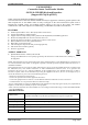
PIN ASSIGNMENT
Interface J3 Pin Assignment
DB9 Signal Direction PCB-J1 Signal
5 GND 1 GND
2 RxD Å Serial data to host 2 TXD1
3 TxD Æ Serial data from host 3 RXD1
4 VCC
Serial Pass-thru or USB data 5 TXD2 (or USB D-)
Serial Pass-thru or USB data 6 RxD2 (or USB D+)
Shield 7 Shield
Extension Port J1 Pin Assignment
Pin Signal Comment
1 GND
2 GND
3 Extended IO
4 Extended IO
5 GND
6 VCC 5Vdc
7 Extended IO
8 Extended IO
9 Extended IO
10 Extended IO
11 Extended IO
12 Extended IO
13 Extended IO
14 Extended IO
15 Extended IO
16 Extended IO
17 Extended IO
18 Extended IO
19 GND
20 VCC_33 3.3V
21 Extended IO
22 Extended IO
23 Extended IO
24 Buzzer Control Signal
25 Extended IO
26 Extended IO
27 Extended IO
28 Extended IO
50 RF Antenna Port J2B Pin Assignment
Contact number Signal
1 RF output
2 GND
Direct Match Antenna Port J2A Pin Assignment
Contact number Signal
1 RX
2 TX
3 GND
4 GND