M-855 Industrial Motherboard User’s Manual Recycled Paper 60070024IHA00
© Copyright 2004 ADLINK Technology Inc. All Rights Reserved. Manual Rev. 1.00: August 16, 2004 The information in this document is subject to change without prior notice in order to improve reliability, design, and function and does not represent a commitment on the part of the manufacturer.
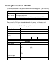
Getting Service from ADLINK Customer Satisfaction is top priority for ADLINK Technology Inc. If you need any help or service, please contact us. ADLINK TECHNOLOGY INC. Web Site http://www.adlinktech.com Sales & Service Service@adlinktech.com TEL Address +886-2-82265877 FAX +886-2-82265717 9F, No. 166, Jian Yi Road, Chungho City, Taipei, 235 Taiwan Please email or FAX your detailed information for prompt, satisfactory, and consistent service.
Table of Contents Chapter 1 Introduction................................................................................. 1 1.1 Unpacking Checklist ................................................................. 2 1.2 Features ..................................................................................... 3 1.3 System Block Diagram ............................................................. 5 1.4 Specifications.............................................................................
1 Introduction The M-855 series combines the high performance and exceptional value of the Intel® 855GME chipset with a full-featured, next generation, industrial board. The Intel® 855GME advanced chipset supports socket 478-pins Intel® Pentium® M processors ranging from 1.30GHz to 1.80GHz, and up to 2GB DDR SDRAM memory on its 400/533MHz FSB.
1.1 Unpacking Checklist 1. Take out the M-855 series unit from the carton box, check if the unit is properly secure in its plastic bag. 2.
¡ Low profile heat sink with fan Note: ¡ I/O Shield M-855 OEM versions with non-standard configurations may vary in function or contents according to request. CAUTION: This board must be protected from static discharge and physical shock. Never remove any of the socketed parts except at a static-free workstation. Use the anti-static bag shipped with the product to handle the board. Wear a wrist strap grounded through one of the system's ESD Ground jacks while servicing system components. ! 1.
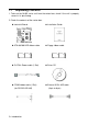
56.05 16.80 29.50 25.42 21.75 6.50 6.22 11.96 38.10 35.97 26.13 21.64 Figure 1: I/O back panel layout M-855 Series Overview Function ¡ Chipset ¡ LVDS ¡ VGA ¡ Gigabit Ethernet ¡ 40-pins EIDE interface ¡ Type II CF socket ¡ Parallel ports ¡ Serial ports ¡ PCI slots ¡ USB 2.
1.3 System Block Diagram Socket 478-pins for Intel Pentium M VRM ADDR CTRL Clock DATA 400/533 MHz FSB LVDS or VGA LCD / CRT Device IDE Primary GMCH (855GME) 732 Micro FCBGA ATA100 DDR266/333 X2 Intel 82541 10/100/1000 Base-TX AC97 Audio Codec IDE Secondary ICH4 421 BGA CF Socket USB2.
1.4 Specifications ¡ Processor: ® ® - Intel Pentium M processor with socket 478-pins package - Processor operating at 1.3GHz and up to 1.8GHz - System bus frequency at 400 / 533 MHz FSB Make sure you use the correct CPU (Pentium® M processor). Using a standard Pentium® 4 CPU may crash the system. ¡ Chipset: - Intel® 855GME + ICH4 AGPset ¡ DRAM Module: - 2 x 184-pin DIMM socket - DDR 266/333 memory - Support DDR SDRAM up to 2GB (max.
¡ Rear I/O Connectors: - PS/2 Mouse and PS/2 style Keyboard - D-Sub 25-pins Printer port connector D-Sub 9-pins COM1 Serial port connector for RS-232 D-Sub 15-pins VGA connector - 2 x USB2.0 connectors - RJ-45 Ethernet and 2 x USB2.0 connectors - Audio for Line-In, Line-Out, MIC phone jack (Optional) ¡ Internal I/O Connectors (pin-header): - 3 x Serial ports, COM2 for RS-232 and COM3 / 4 for RS-232/422/485 (Serial cable with bracket) - 2 x USB2.
2 Installation 2.1 System Installation CPU Installation Carefully follow the steps below to install the CPU: 1. Check and confirm that the jumpers are correctly set for the CPU you are going to install (figure 3). 2. Take the screwdriver and releasing screw-nut of the Socket 478. 3. Rotate mark of screw-nut to face the “OPEN”. 4. Align the pins of the CPU against the pinholes of the Socket 478. Be sure to pay attention to the orientation of the CPU.
8. Push down the opposite side of the ZIF clip and hook it. 9. Connect the cooling fan cable to the socket as shown below. Be careful not to place the cable on the CPU cooling fan. Removing a CPU: 1. Before removing the CPU, turn off the power and wait for about 20 minutes until the heat radiation plate of the cooling fan and the CPU cools down. 2. Rotate mark of screw-nut to face the “OPEN”. 3. To remove the CPU. WARNING: The CPU and the heat radiation plate are hot and can cause burns.
Figure 5 display the notch marks and what they should look like on your DIMM memory module. DIMMs have184 pins and two notches that will match with the onboard DIMM socket. DIMM modules are installed by placing the chip firmly into the socket at a 90-degree angle and pressing straight down (figure 6) until it fits tightly into the DIMM socket. Figure 5: DIMM Memory and 184-pins Socket Figure 6: Memory Installation Carefully follow the steps below in order to install the DIMMs: 1.
To remove the DIMM, use your fingers or a small screwdriver to carefully push away the plastic tabs that secure the DIMM at each end. Lift it out of the socket. Make sure you store the DIMM in an anti-static bag. Only use the same size and manufacturer of memory modules. Setting Jumpers and DIP Switches There are jumpers and DIP-switches on the M/B of the M-855 Series. The jumpers can be set for various operations.
2.
2.3 Jumper Settings Jumper Location Description: Use the information in the following table to change the jumpers and the DIP switches. Jumpers JP1 JP2 JP3 JP4 JP5 JP6 Functions COM3 Port Setting Select COM4 Port Setting Select CPU Type Setting Select Watchdog Timer Setting Select Clear CMOS Setting Select Power Management Setting Select A description on setting the jumpers to enable/disable or change functions is illustrated below. Please refer to the diagrams below for jumper locations.
CPU Type Setting Select: JP3 Function JP3 CPU FSB 400 MHz (Default) 1-2 On CPU FSB 533 MHz 1-2 Off y Location: Watchdog Timer Setting Select: JP4 Function JP4 NMI 1-2 Reset System (Default) 2-3 Clear CMOS Setting Select: JP5 Function JP5 y Location: Normal (Default) 1-2 Clear CMOS 2-3 y Location: Installation • 15
Power Management Setting Select: JP6 Function JP6 ACPI Mode On APM Mode (Default) Off y Location: 2.
Table for Connector’s Location Description: Use the information in the following table to change the connector.
CRT VGA Port Connector (D-SUB 15-pins Female): CN1 Pin # Assignment Pin # Assignment 1 Red 2 Green 3 Blue 4 NC 5 Ground 6 Ground 7 Ground 8 Ground 9 VCC 10 Ground 11 NC 12 DData 13 HSync 14 VSync 15 DCK y Figure: 5 1 15 11 COM1 RS-232 Serial Port Connector (D-Sub 9-pins Male): CN2 Pin # Assignment Pin # Assignment 1 DCD (Data Carrier Detect) 6 DSR (Data Set Ready) 2 RXD (Receive Data) 7 RTS (Request to Send) 3 TXD (Transmit Data) 8 CTS (Clear to Send) 4 DTR (Da
Parallel Port Connector (D-Sub 25-pins Male): CN3 Pin # Assignment Pin # Assignment 1 Line Printer Strobe 14 2 PD 0, Parallel Data 0 15 Auto Feed Error 3 PD 1, Parallel Data 1 16 Initialize 4 PD 2, Parallel Data 2 17 Select 5 PD 3, Parallel Data 3 18 Ground 6 PD 4, Parallel Data 4 19 Ground 7 PD 5, Parallel Data 5 20 Ground 8 PD 6, Parallel Data 6 21 Ground 9 PD 7, Parallel Data 7 22 Ground 10 ACK, Acknowledge 23 Ground 11 Busy 24 Ground 12 Paper Empty 25 Grou
Audio Port Connector (Audio Phone–Jack): CN5 (Optional) Pin # Assignment BLUE Line-In GREEN Line-Out Red Mic-In y Figure: Blue Green Red PS/2 Keyboard Connector (6-pins Green Mini Din): CN6 Pin # Assignment Pin # Assignment 1 Keyboard Data 2 NC 3 Ground 4 +5V 5 Keyboard Clock 6 NC y Figure: 6 5 4 3 2 1 PS/2 Mouse Connector (6-pins Purple Mini Din): CN6 Pin # Assignment Pin # Assignment 1 Mouse Data 2 NC 3 Ground 4 +5V 5 Mouse Clock 6 NC y Figure: 6 5 4 3 2 20 •
Gigabit Ethernet RJ-45 Connector (RJ-45 Phone–Jack): CN7 Pin # Assignment Pin # Assignment 1 Transmit output (+) 5 NC 2 Transmit output (-) 6 Receive input (-) 3 Receive input (+) 7 NC 4 NC 8 NC y Figure: USB 2/3 Connector (4-pins Female): CN7 Pin # Assignment Pin # Assignment 1a VCC 1b VCC 2a USB2 - 2b USB3 - 3a USB2 + 3b USB3 + 4a Ground 4b Ground y Figure: 1 4 1 4 External Keyboard & Mouse Connector (6-pins Pin-Header): CN8 Pin # Assignment Pin # Assignment 1 MS
CD_IN Connector: CN9 Pin # Assignment 1 CD_IN_Left 2 CD_GND 3 CD_GND 4 CD_IN_Right y Figure: 4 1 COM3 RS-232/422/485 Serial Port Connectors (14-pins Pin-Header): CN13 Pin # Assignment Pin # Assignment 1 DCD 2 RXD 3 TXD 4 DTR 5 Ground 6 DSR 7 RTS 8 CTS 9 RI 10 Ground 11 TXD+ 12 TXD- 13 RXD+ 14 RXD- y COM3 Figure: 22 • Installation 14 13 2 1
COM4 RS-232/422/485 Serial Port Connectors (14-pins Pin-Header): CN14 Pin # Assignment Pin # Assignment 1 DCD 2 3 TXD 4 RXD DTR 5 Ground 6 DSR 7 RTS 8 CTS 9 RI 10 Ground 11 TXD+ 12 TXD- 13 RXD+ 14 RXD- y COM4 Figure: 14 13 2 1 Note: How to connect a RS485 device with the COM port ribbon cable? Our Industrial Board encloses a COM port ribbon cable for internal connection. RS422/485 device must connect to downside D-Sub with 5-pin cable and signal indication as below.
CPU Fan Power Connector: CN15 Pin # Assignment 1 Ground 2 VCC 3 Fan Status Signal y Figure: 3 1 COM2 RS-232 Serial Port Connector (10-pins Pin-Header): CN16 Pin # Assignment Pin # Assignment 1 DCD 2 DSR 2 RXD 4 RTS 3 TXD 6 CTS 4 DTR 8 RI 5 Ground 10 Ground y Figure: 10 9 2 1 18/24 Bits LVDS Panel Interface (40-pins Male): CN17 Pin # Assignment Pin # Assignment 1 NC 2 NC 3 Ground 4 Ground 5 YAM0 6 YAM1 7 YAP0 8 YAP1 9 Ground 10 Ground 11 YAM2 12 CLKA
21 Ground 22 Ground 23 25 YBM1 24 YBM2 YBP1 26 YBP2 27 Ground 28 Ground 29 CLKBM 30 YBM3 31 CLKBP 32 YBP3 33 NC 34 +12V 35 NC 36 +12V 37 NC 38 PVCC 39 BKL 40 PVCC y Figure: System Fan Power Connector: CN18 Pin # 1 40 2 39 1 Assignment Ground 2 VCC 3 Fan Status Signal y Figure: 1 3 Installation • 25
USB 4/5 Connector (9-pins Pin-Header): CN19 Pin # Assignment Pin # 1 Assignment VCC 2 VCC 3 USB4 - 4 USB5 - 5 USB4 + 6 USB5 + 7 Ground 8 Ground 9 --- 10 NC y Figure: 2 10 1 9 System Panel Indicate Connector: CN20 Pin # Assignment Pin # SPEAKER 1 +5V Assignment PWR LED 2 PWLED+ 3 NC 4 NC 5 BUZZER 6 PWLED- 7 KEYLOCK SPEAKER HDD LED 8 KBLOCK Ground 9 HDLED+ 10 11 HDLED- 12 NC RESET PWR ON 13 RESET+ 14 PWRBT+ 15 RESET- 16 PWRBT- y Figure: 26 • Instal
Secondary IDE Connector (40-pins 2.
ATX Power Connector: CN22 Pin # Assignment Pin # Assignment +3.3V 11 +3.3V 2 +3.3V 12 -12V 3 Ground 13 Ground 4 +5V 14 PS-ON 5 Ground 15 Ground 6 +5V 16 Ground 7 Ground 17 Ground 8 NC 18 -5V 9 5VSB 19 +5V 10 +12v 20 +5V 1 y Figure: 1 10 11 20 Primary IDE Connector (40-pins 2.
Address 0 36 Address 2 37 39 Chip Select 0 38 Chip Select 1 Activity 40 Ground y Figure: 2 40 1 39 Floppy Disk Connector (34-pins 2.
LINE OUT Connector: CN25 Pin # Assignment 1 LOUT_L 2 AU_GND 3 VCC_5V 4 LOUT_R y Figure: 4 1 LAN LED Connector: JP7 Pin # Assignment Pin # Assignment 1 LINK_LED 2 VCC_3V 3 ACT_LED 4 VCC_3V y Figure: 1 2 3 4 30 • Installation
S-ATA1 Connector (9-pins): SATA1 Pin # Assignment 1 Ground 2 SATA1_TXP 3 SATA1_TXN 4 Ground 5 SATA1_RXN 6 SATA1_RXP 7 Ground 8 Ground 9 Ground y Figure: 91 S-ATA2 Connector (9-pins): SATA2 Pin # 78 Assignment 1 Ground 2 SATA2_TXP 3 SATA2_TXN 4 Ground 5 SATA2_RXN 6 SATA2_RXP 7 Ground 8 Ground 9 Ground y Figure: 91 78 Installation • 31
Type II CompactFlash™ Connector: CF II Pin # Assignment Pin # Assignment 1 Ground 2 D3 3 D4 4 D5 5 D6 6 D7 7 CS#1 8 Ground 9 Ground 10 Ground 11 Ground 12 Ground 13 VCC 14 Ground 15 Ground 16 Ground 17 Ground 18 A2 19 A1 20 A0 21 D0 22 D1 23 D2 24 NC 25 NC 26 NC 27 D11 28 D12 29 D13 30 D14 31 D15 32 CS#3 33 NC 34 IOR# 35 IOW# 36 VCC 37 INTS 38 VCC 39 CSEL# 40 NC 41 IDERST# 42 IORDY 43 NC 44 VCC 45 IDEACTS# 46 DET 4
3 Award BIOS Setup 3.1 BIOS Instructions Award’s ROM BIOS provides a built-in Setup program, which allows the user to modify the basic system configuration and hardware parameters. The modified data will be stored in a battery-backed CMOS, so that data will be retained even when the power is turned off. In general, the information saved in the CMOS RAM will stay unchanged unless there is a configuration change in the system, such as hard drive replacement or a device is added.
Phoenix - AwardBIOS CMOS Setup Utility ¾Standard CMOS Feature ¾Frequency/Voltage Control ¾Advanced BIOS Feature Load Fail-Safe Defaults ¾Advanced Chipset Feature Load Optimized Defaults ¾Integrated Peripherals Set Supervisor Password ¾Power Management Setup Set User Password ¾PnP/PCI Configurations Save & Exit Setup ¾PC Health Status Exit Without Saving Esc: Quit ↑ ↓ ← →: Select Item F10: Save & Exit Setup Time, Date, Hard Disk Type….
Use this menu to show your system temperature, speed and voltage status. See 3.10 for the details. Frequency / Voltage Control: Use this menu to specify your settings for frequency/voltage control. See 3.11 for the details. Load Fail-Safe Defaults: Use this menu to load the BIOS default values for the minimal/stable performance for your system to operate. See 3.12 for the details.
Standard CMOS Features Mon, JUN 7 2004 Item Help 16:19:20 ____________________________ Date (mm:dd:yy): Time (hh:mm:ss): ¾ IDE Primary Master ¾ IDE Primary Slave ¾ IDE Secondary Master ¾ IDE Secondary Slave 13579 MB None None None Drive A Drive B 1.44M, 3.5 in.
Video: Options EGA/VGA/CGA 40/CGA 80/MONO Select the default video device. Halt On: Options All Errors/No Errors/All, All but Keyboard/All, All but Diskette/All, All but Disk/Key Select the situation in which you want the BIOS to stop the POST process and notify you. Base Memory: Option N/A Displays the amount of conventional memory detected during boot up. Extended Memory: Option N/A Displays the amount of extended memory detected during boot up.
IDE Primary Master: Options None, Auto and Manual Selecting “Manual” lets you set the remaining fields on this screen. Selects the type of fixed disk. "User Type" will let you select the number of cylinders, heads, etc. Note: PRECOMP=65535 means NONE! Access Mode: Options CHS, LBA, Large and Auto Choose the access mode for this hard disk Capacity: Options Auto Display your disk drive size Disk drive capacity (Approximated).
3.5 Advanced BIOS Features This section allows you to configure your system for basic operation. You have the opportunity to select the system’s default speed, boot-up sequence, keyboard operation, shadowing and security.
Hard Disk Boot Priority: Press Enter and It shows Bootable add-in Card. Virus Warning: Allow you to choose the VIRUS Warning feature for IDE Hard Disk boot sector protection. If this function is enabled and someone attempts to write data into this area, BIOS will show a warning message on screen and alarm beep. Enabled---Activates automatically when the system boots up causing a warning message to appear when anything attempts to access the boot sector or hard disk partition table.
Boot Up Floppy Seek: Seeks disk drives during boot up. Disabling speeds boot up. The choices: Enabled, Disabled. Boot Up NumLock Status: Select power on state for NumLock. The choices: On, Off Gate A20 Option: Select if chipset or keyboard controller should control GateA20. Normal---A pin in the keyboard controller controls GateA20 Fast---Lets chipset control GateA20 Typematic Rate Setting: Keystrokes repeat at a rate determined by the keyboard controller.
Select the operating system that is running with greater than 64MB of RAM on the system. The choices: Non-OS2, OS2. Report No FDD For Win 95: Whether report no FDD for Windows 95 or not. The choices: Yes, No. 3.6 Advanced Chipset Features This section allows you to configure the system based on the specific features of the installed chipset. This chipset manages bus speeds and access to system memory resources, such as DRAM and the external cache.
Select the operating system that is selecting DRAM timing, so select SPD for setting SDRAM timing by SPD. The choices: Manual, By SPD. CAS Latency Time: When synchronous DRAM is installed, the number of clock cycles of CAS latency depends on the DRAM timing. The choices: 2, 2.5. Active To Precharge Delay: Select the operating system that is active to precharge delay. The choices: 5, 6, 7.
The choices: Enabled, Disabled. Video BIOS Cacheable: Select “Enabled” allows caching of the video BIOS, resulting in better system performance. However, if any program writes to this memory area, a system error may result. The choices: Enabled, Disabled. Memory Hole At 15M-16M: You can reserve this area of system memory for ISA adapter ROM. When this area is reserved, it cannot be cached.
The choices: VBIOS Default, CRT, LFP and CRT+LEP. Panel Number: This item allows you to select the panel resolution. The choices: 1-8. 3.
OnChip Primary/Secondary PCI IDE: The integrated peripheral controller contains an IDE interface with support for two IDE channels. Select “Enabled” to activate each channel separately. The choices: Enabled, Disabled. IDE Primary/Secondary Master/Slave PIO: The four IDE PIO (Programmed Input/Output) fields let you set a PIO mode (0-4) for each of the four IDE devices that the onboard IDE interface supports. Modes 0 through 4 provide successively increased performance.
USB Keyboard Support: Select “Enabled” if your system contains a Universal Serial Bus (USB) controller and you have a USB keyboard. The choices: Enabled, Disabled. USB Mouse Support: Select “Enabled” if your system contains a Universal Serial Bus (USB) controller and you have a USB mouse. The choices: Enabled, Disabled. AC97 Audio: This item allows you to decide to auto or disable the chipset family to support AC97 Audio. The choices: Auto, Disabled.
KB Power ON Password: You can use this item to limit operating KB Power On system. The choice: Enter Hot Key Power ON: You can use this item to select operating Hot Key to Power On system. The choices: Ctrl-F1~Ctrl-F12. Onboard FDC Controller: Select “Enabled” if your system has a floppy disk controller (FDC) installed on the system board and you wish to use it. If you install and-in FDC or the system has no floppy drive, select Disabled in this field. The choices: Enabled, Disabled.
Onboard Serial Port 1/Port 2: Select an address for the first and second serial ports. Serial Port 1/Port 2 Use IRQ: Select an IRQ for the first and second serial ports. Onboard Serial Port 3/Port 4: Select an address for the third and forth serial ports. Serial Port 3/Port 4 Use IRQ: Select an IRQ for the third and forth serial ports. 3.
This item allows you to enable or disable the Advanced Configuration and Power Management (ACI). The choices: Enabled, Disabled. Power Management: This category allows you to select the type (or degree) of power saving and is directly related to the following modes: 1. HDD Power Down 2. Doze Mode 3. Suspend Mode Min. Power Saving: Minimum power management. Doze Mode = 1 hr., Standby Mode = 1 hr., Suspend Mode = 1 hr., and HDD Power Down = 15 min. Max.
Suspend Type: Select the Suspend Type. The choices: PWRON Suspend, Stop Grant. Suspend Mode: When “Enabled” and after the set time of system inactivity. All devices except the CPU will be shut off. The choices: Enabled, Disabled. HDD Power Down: When “Enabled” and after the set time of system inactivity, the hard disk drive will be powered down while all other devices remain active. The choices: Enabled, Disabled. CPU THER-Throttling: Select the CPU THRM-Throttling rate. The choices: 12.5%, 25.0%, 37.
3.9 PnP/PCI Configurations This section describes configuring the PCI bus system. PCI, or Personal Computer Interconnect, is a system that allows I/O devices to operate at speeds nearing the speed the CPU itself uses when communicating with its own special components. This section covers some very technical items and it is strongly recommended that only experienced users should make any changes to the default settings.
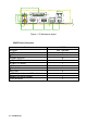
3.10 PC Health Status Phoenix - AwardBIOS CMOS Setup Utility PC Health Status CPU Warning Temperature SYS Temperature CPU Temperature CPU FAN SYSFAN VDIMM VCORE +3.3 +5V +12 V -12 V -5V VBAT (V) 5VSB (V) Shutdown Temperature Disabled 32°C / 89°F 28°C / 82°F 5152RPM 3283RPM 2.48 4.42V 3.34V 4.94V 11.85V -12.28V -4.99V 3.02V 5.
+3.3V/+5V/+12V/-12V/-5V/5VSB(V): Displays the voltage of +5V/+12V/-12V/-5V. VBAT (V): Displays the voltage level of the battery. Shutdown Temperature: This item allows you to set up the CPU shutdown Temperature. This item is only effective under Windows® 98 ACPI mode. The choices: Disabled, 60°C / 140°F, 65°C / 149°F, 70°C / 159°F and 75°C / 167°F. 3.
Load Fail-Safe Defaults (Y/N)? N Pressing ‘Y’ loads the BIOS default values for the most stable, minimal-performance system operations. 3.13 Load Optimized Defaults When you press on this item you get a confirmation dialog box with a message similar to: Load Optimized Defaults (Y/N)? N Pressing ‘Y’ loads the default values that are factory settings for optimal performance system operations. 3.14 Supervisor/User Password Setting You can set either supervisor or user password, or both of then.
PASSWORD DISABLED. When a password has been enabled, you will be prompted to enter it every time you try to enter Setup. This prevents an unauthorized person from changing any part of your system configuration. Additionally, when a password is enabled, you can also require the BIOS to request a password every time your system is rebooted. This would prevent unauthorized use of your computer.
Warranty Policy Thank you for choosing ADLINK. To understand your rights and enjoy all the after-sales services we offer, please read the following carefully. 1. Before using ADLINK’s products please read the user manual and follow the instructions exactly. When sending in damaged products for repair, please attach an RMA application form which can be downloaded from: http://rma.adlinktech.com/policy/. 2. All ADLINK products come with a limited two-year warranty, one year for products bought in China.