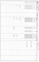
Appendices FIGURE 8-F – EXCITER BLOCK DIAGRAM IC 3 MOD. AMP 8A15218 150U2 174 MHz VCO-2 Q4 DOUBLLER 151-174MHz 2SC3356 Q3 AMPLIFIER 2SC3356 Q2 AMPLIFIER 2SC3356 Q6 KEY CONT. 2SA1052 Q7 CONTROL 2SA1244 Q1 AMPLIFIER 2SC3356 J2 OUTPUT LPF 150 - 174 MHz LOOP FILTER Q22,Q23 SWEEP RL1P141C RT1N441C Q26,Q27 CHARGE PUMP 2SA1052 2SC2462 +5V Q5 AMPLIFIER 2SC3585 Q24 RIPPLE FIL 2SC2462 IC 4 PLL MB1504 Q8 AMPLIFIER FMW.1 D1 DETECTOR HSM107S RV3 POWER SET Q25 LOCK DET RT1N441C Q20 IF AMP.
Appendices FIGURE 8-G – EXCITER BOARD ALIGNMENT PROCEDURE 1. Connection Connect the cables from RF unit to J1 (signal and power source), J3 (10.7 MHz) and J4 (10 MHz). Connect a modulation analyzer to J2 (output). 2. Alignment 2-1 VCO 2-1-1. Use a PLL data of the frequency that is actually used for data transmission. Turn power on. While monitoring TP1, adjust the core of the channel VCO for approximately 4V. 2-1-2. While monitoring TP2, adjust the modulation VCO for approximately 4V. 2-2 Modulation 2-2-1.
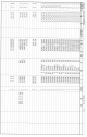
Appendices FIGURE 9 – FREQUENCY DATA STREAM FREQUENCY DATA STREAM 1. PROGRAMMABLE REFERENCE COUNTER MSB 0 LSB 0 0 1 0 0 0 0 0 0 0 0 0 0 0 1 PGM DATA PGM CLOCK 4094 STRB PLL STRB 2.
Appendices FIGURE 9 – FREQUENCY DATA STREAM CONT’D FREQUENCY DATA STREAM 2 1. PROGRAMMABLE REFERENCE COUNTER MSB 0 LSB 0 0 1 0 0 0 0 0 0 0 0 0 0 0 1 PGM DATA PGM CLOCK 4094 STRB PLL STRB 2.
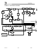
Appendices FIGURE 10 – PLL BLOCK DIAGRAM T.C.X.O 10.7 MHz MOUDULATED CARRIER 1/NR EEPROM P/D CPU P/C S/C CH-SW 1/NP PRA-SCA CHARGE PUMP L.P.F. V.C.
Appendices FIGURE 11 - MATHCAD ENCO synthesizer setup bit values 3FLX150SU.MCD 4-17-02 HAV "Calculate the binary values to load for the Ft-10.7 Mhz loop" . 6 156.210 fdes1 6 10.7. 10 fdes1 fdesnt1 steps PSV1 7500 64 fdesr1 steps fref floor steps 4 fdesnt1 = 1.94 10 fdesr1 = 400 fdesnt1 PSV1 fdesn1 3. 106 fref fdesr1. 2 bvr1 1 fdesn1 = 303.125 If Prescaler =32 then set 2^15 n1 floor( fdesn1 ) n1 = 303 a1 ( fdesn1 n1 ) .PSV1 bvr1 if PSV1 32, 0 , 215 fdesr1.2 1 a1 = 8 bvf1 8 n1.
Appendices LIST 1 – EXTEND-A-PAGE TRANSMITTER REAR PANEL CONNECTOR DESCRIPTION L.1 Extend-A-Page Transmitter Unit System Interface Connector (DB9 to P5 Connector on Motherboard) Db9 Pin # Description 1 2 3 4 5 6 7 8 9 – Analog Key (Active Low) – Audio + – Audio – Digital Key (Active Low) – Digital Data (TTL or RS232) – D-Reset (Active High) – Hotkey (Active Low) – +12VDC Output – Ground NOTES: 1. Both Digital and Analog Key inputs accepts TTL level ‘Low’ or Form C relay closure to ground. 2.
Appendices LED DESCRIPTION – FRONT PANEL LEDS Version 4 AKEY DKEY SYS DATA POWER Indicates Transmitter Keyed in Analog Mode Indicates Transmitter Keyed in Digital Mode GREEN – System Ready Indicates Presence of Analog/Digital Data Indicates Presence of System AC Power A-55 4/2/04
Appendices Report 1 – Extend-A-Page Malfunction Report RMA No. __________ Date Rec’d: ________________ Model No. _________ Serial No. _______________ Date Returned: _____________ 1. Describe Malfunction: __________________________________________________ ______________________________________________________________________ ______________________________________________________________________ 2. Total Number of Operating Hours: ________________________________________ 3.
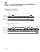
150 MHz Exciter Label 1. Label Drawing 2.
ocxo_1.
ocxo_2.
ocxo_3.
PRODUCT NAME: VHF Extend-A-Page Transmitter MODEL: VEP-02T APPLICANT / MANUFACTURER: Eagle Wireless International, Inc 101 Courageous Drive League City, TX 77573