
Schematics
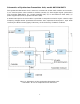


Figure 2. Schematics of the Triple DDS Radar Controller.
See Table 2 for list of components and references.
Figure 3. Photo of the Triple DDS Radar Controller board.
2
SXLP-30+
Filter
Driver
SXLP-30+
Filter
Driver
AD9512
Secondary
Clock
Buffer /
Divider
IOUD/BPSK / OSK
AD9854
DDS
A
SXLP-30+
Filter
Driver
SXLP-30+
Filter
Driver
OCXO
SXLP-30+
Filter
AD9854
DDS
C
Clock
Remap
AD9854
DDS
B
AD9512
Primary
Clock
Buffer /
Divider
CLK
IN
SPI
SPI
I
OUT
Q
OUT
I
OUT
Q
OUT
SPI
IOUD/BPSK / OSK
MCX Cable Connector Logic Connection with FPGA
KEY