
User's Manual

8
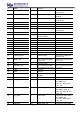
SPI
SPI interface
Input DC voltage at SPI interface pin
-0.3V
3.6V
GPS_PPS
GPS PPS input
Input DC voltage at GPS_PPS input
pin
-0.3V
3.6V
Pho_ANT
Antenna ruggedness
Output RF load mismatch
ruggedness at ANT1
10:1
VSWR
Tstg
Storage temperature
-40 °C
85 °C
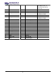
WARNING:
The product is not protected against overvoltage or reversed voltages. If necessary, voltage spikes
exceeding the power supply voltage specification, given in table above, must be limited to values
within the specified boundaries by using appropriate protection devices
Maximum ESD
Parameter
Min
Typical
Max
Remarks
ESD_HBM
1000V
Charged Device Model JESD22-C101 CLASS III
ESD_CDM
1000V
Charged Device Model JESD22-C101 CLASS III
NOTE:
Although this module is designed to be as robust as possible, electrostatic discharge (ESD) can
damage this module. This module must be protected at all times from ESD when handling or
transporting. Static charges may easily produce potentials of several kilovolts on the human body
or equipment, which can discharge without detection. Industry-standard ESD handling precautions
should be used at all times.
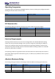
Power Consumption
Mode
Condition
Min
Typical
Max
Active mode (TX)
The power of the TX channel is 20 dBm and
3.3V supply.
511mA
512mA
513mA
Active mode (RX)
TX disabled and RX enabled
70mA
81.6mA
101mA
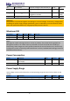
Power Supply Range
Input voltage at 3V3 must be above the normal operating range minimum limit to switch on the
module.
Symbol
Parameter
Min
Typical
Max
3V3
Module supply operating input voltage
3V
3.3V
3.6V