
User's Manual

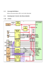
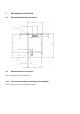
Table of Contents
CDMRF101...........................................................................................................................................................1
TCU PHONE MODULE........................................................................................................................................1
1 INTRODUCTION / OVERVIEW...................................................................................................................6
1.1 MSM 6050 Chipset .................................................................................................................................6
1.1.1 MSM 6050 Features........................................................................................................................6
1.2 IS- Mobile Standards .............................................................................................................................7
1.3 Acronym Definitions..............................................................................................................................8
1.4 Development Tools for the Phone Module..........................................................................................8
1.4.1 LT Box.............................................................................................................................................8
.....................................................................................................................................................................8
2 MECHANICAL DESCRIPTION ...................................................................................................................9
2.1 Phone Module Mechanical Outline ......................................................................................................9
2.2 Phone Module I/O Connector ...............................................................................................................9
2.2.1 I/O Connector Drawing and Supplier Part Number......................................................................... 9
2.2.2 I/O Connector Electrical Characteristics .......................................................................................10
2.2.2.1 I/O Connector Pin Assignment ..............................................................................................10
3 OPERATING TEMPERATURE AND STORAGE .....................................................................................13
3.1 Temperature.........................................................................................................................................13
3.1.1 Storage Temperature.................................................................................................................... 13
3.1.2 Operating Temperature.................................................................................................................13
4 ELECTRICAL INTERFACE.......................................................................................................................14
4.1 Design Guidelines ...............................................................................................................................14
4.1.1 Component Derating.....................................................................................................................14
4.1.1.1 Ceramic Capacitors / Parallel Plate Capacitors..................................................................... 14
4.1.1.2 Electrolytic Capacitors ...........................................................................................................14
4.1.1.3 Tantalum Capacitors..............................................................................................................14
4.1.2 Communication Pins and Unused Pins......................................................................................... 14
4.2 Supply Voltage.....................................................................................................................................14