
Specification Sheet

5
www.v-color.com.tw
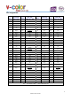
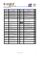
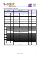
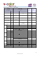
Pin Descriptions
Pin Name
Description
Num
ber
Pin Name
Description
Num
ber
CK0
Clock Input, positive line
1
ODT[1:0]
On Die Termination Inputs
2
CK0
Clock Input, negative line
1
DQ[63:0]
Data Input/Output
64
CK1
Clock Input, positive line
1
CB[7:0]
Data check bits Input/Output
8
CK1
Clock Input, negative line
1
DQS[8:0]
Data strobes
9
CKE[1:0]
Clock Enables
2
DQS[8:0]
Data strobes, negative line
9
RAS
Row Address Strobe
1
DM[8:0]/
DQS[17:9],
TDQS[17:9]
Data Masks / Data strobes,
Termination data strobes
9
CAS
Column Address Strobe
1
DQS[17:9],
TDQS[17:9]
Data strobes, negative line,
Termination data strobes
9
WE
Write Enable
1
EVENT
Reserved for optional hardware
temperature sensing
1
S[3:0]
Chip Selects
4
TEST
Memory bus test tool (Not Con
nected and Not Usable on DIMMs)
1
A[9:0],A11,
A[15:13]
Address Inputs
14
RESET
Register and SDRAM control pin
1
A10/AP
Address Input/Autoprecharge
1
VDD
Power Supply
22
A12/BC
Address Input/Burst chop
1
VSS
Ground
59
BA[2:0]
SDRAM Bank Addresses
3
VREFDQ
Reference Voltage for DQ
1
SCL
Serial Presence Detect (SPD)
Clock Input
1
VREFCA
Reference Voltage for CA
1
SDA
SPD Data Input/Output
1
VTT
Termination Voltage
4
SA[2:0]
SPD Address Inputs
3
VDDSPD
SPD Power
1
Par_In
Parity bit for the Address and
Control bus
1
Err_Out
Parity error found on the
Address and Control bus
1