
Specification Sheet


12
www.v-color.com.tw
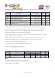
Speed Bin Table Notes
Absolute Specification
- VDDQ = VDD = 1.20V +/- 0.06 V
- VPP = 2.5V +0.25/-0.125 V
- The values defined with above-mentioned table are DLL ON case.
- DDR4-1600, 1866, 2133 and 2400 Speed Bin Tables are valid only when Geardown Mode is
disabled.
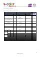
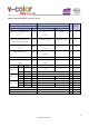
1. The CL setting and CWL setting result in tCK(avg).MIN and tCK(avg).MAX requirements.
When making a selection of tCK(avg), both need to be fulfilled: Requirementsfrom CL setting
as well as requirements from CWL setting.
2. tCK(avg).MIN limits: Since CAS Latency is not purelyanalog - data and strobe output are
synchronized by the DLL - all possible intermediate frequencies may not be guaranteed. An
application should use the next smaller JEDEC standard tCK(avg) value (1.5, 1.25, 1.071,
0.938 or 0.833 ns) when calculating CL [nCK] = tAA [ns] / tCK(avg) [ns], rounding up to the
next ‘Supported CL’, where tAA = 12.5ns and tCK(avg) = 1.3 ns should only be used for CL =
10 calculation.
3. tCK(avg).MAX limits: Calculate tCK(avg) = tAA.MAX / CL SELECTED and round the
resulting tCK(avg) down to the next valid speed bin (i.e. 1.5ns or 1.25ns or 1.071 ns or 0.938
ns or 0.833 ns). This result is tCK(avg).MAX corresponding to CL SELECTED.
4. ‘Reserved’ settings are not allowed.User must program a different value.
5. 'Optional' settings allow certain devices in the industry to support this setting, however, it is
not a mandatory feature. Refer to supplier's data sheet and/or the DIMM SPD information if
and how this setting is supported.
6. Any DDR4-1866 speed bin also supports functional operation at lower frequencies as shown
in the table which are not subject to Production Tests but verified by Design/Characterization.
7. Any DDR4-2133 speed bin also supports functional operation at lower frequencies as shown
in the table which are not subject to Production Tests but verified by Design/Characterization.