
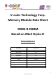
Specification Sheet


6
www.v-color.com.tw
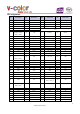
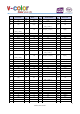
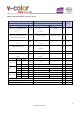
Pin Descriptions
Pin Name
Description
Pin Name
Description
A0-A171
Register address input
SCL
I2C serial bus clock for SPD-TSE and
register
BA0, BA1
Regisiter bank select input
SDA
I2C serial data line for SPD-TSE and
register
BG0, BG1
Regisiter bank group select input
SA0-SA2
I2C slave address select for SPD-TSE
and register
RAS_n2
Register row address strobe input
PAR
Register parity input
CAS_n3
Register column address strobe input
VDD
SDRAM core power supply
WE_n4
Register write enable input
C0, C1, C2
Chip ID lines for SDRAMx
CS0_n, CS1_n,
CS2_n, CS3_n
DIMM Rank Select Lines input
12V
Optional Power Supply on socket but
not used on RDIMM
CKE0, CEK1
Register clock enable lines input
VREFCA
SDRAM command/address reference
supply
ODT0, ODT1
Register on-die termination control
lines input
VSS
Power supply return (ground)
ACT_n
Register input for activate input
VDDSPD
Serial SPD/TS positive power supply
DQ0-DQ63
DIMM memory data bus
ALERT_n
Register ALERT_n output
CB0-CB7
DIMM ECC check bits
VPP
SDRAM Supply
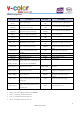
TDQS9_t-TDQS17_t
TDQS9_c-TDQS17_c
Dummy loads for mixed populations of
x4 based and x8 based RDIMMs.
DQS0_t-DQS17_t
Data Buffer data strobes
(positive line of differential pair)
DM0_n-DM8_n
Data Mask
DQS0_c-DQS17_c
Data Buffer data strobes
(negative line of differential pair)
RESET_n
Set Register and SDRAMs to a Known
State
DBI0_n-DBI8_n
Data Bus Inversion
EVENT_n
SPD signals a thermal event has
occurred
CK0_t, CK1_t
Register clock input (positive line of dif-
ferential pair)
VTT
SDRAM I/O termination supply
CK0_c, CK1_c
Register clocks input (negative line of
differential pair)
RFU
Reserved for future use
1. Address A17 is only valid for 16Gbx4 based SDRAMs.
2. RAS_n is a multiplexed function with A16.
3. CAS_n is a multiplexed function with A15.
4. WE_n is a multiplexed function with A14.