Assembly instructions User guide
Manuals
Brands
Velleman projects Manuals
Hardware
K1803
1
2
3
4
5
6
7
8
7
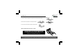
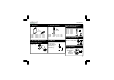
9. Schem
atic diagra
m
.
Sch
em
at
ic di
agram
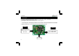
&
P
CB
R4
10
0K
R3
10
0K
R2
100K
C1
10µ
GN
D
+V
C2
10
µ
C5
10
µ
SK1
AF
I
N
SK
2
AF
O
UT
3
2
8
4
1
IC1
A
5
6
7
IC
1
B
C3
10µ
C4
10µ
R7
2K2
R6
100K
R1
100K
R5
100K
RV1
22
0K
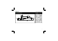
10. PCB
1
...
...
5
6
7
8