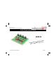
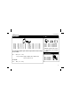
Total solder points: 108 Difficulty level: beginner 1 2 3 4 5 advanced QUAD TRIAC SWITCH CARD K2634 cuits ower cir .
Features & Specifications Applying relays is the most usual way to switch an alternating current (AC) with an electronic control, because of its simplicity and its security, as the switching and switched voltage are completely separated. The low speed (esp. for illuminated advertisements ) and the short life of the contacts are however major disadvantages. In order to avoid the disadvantages of the relay without losing the advantages, optocoupler controlled triacs are used.
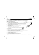
Assembly hints 1. Assembly (Skipping this can lead to troubles ! ) Ok, so we have your attention. These hints will help you to make this project successful. Read them carefully. 1.1 Make sure you have the right tools: • A good quality soldering iron (25-40W) with a small tip. • Wipe it often on a wet sponge or cloth, to keep it clean; then apply solder to the tip, to give it a wet look. This is called ‘thinning’ and will protect the tip, and enables you to make good connections.
Assembly hints 1.
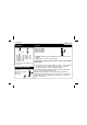
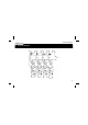
Construction 2 . IC’s. 1. Resistors R...
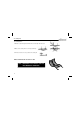
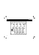
Construction 4. PCB tabs 6. Triacs TRI1 : TIC206M TRI2 : TIC206M TRI3: TIC206M TRI4 : TIC206M VAC OUT1 OUT2 OUT3 OUT4 9VDC : 2X : 2X : 2X : 2X : 2X : 2X IN1 IN2 IN3 IN4 : 2X : 2X : 2X : 2X Remarks : Make sure the metal backside of the triacs points to the outputs. Apply a layer of tin on the entire PCB track. You can also use terminal connectors. 5. LED. Watch the polarity! LD1 LD2 LD3 LD4 5mm Red LD1 CATHODE 6 TR... If you want to switch more than 1,5A per output, then the triacs need cooling.
Connection 7. Connection Connect the minus side of the inputs to the open collector outputs of the interface card(s) (see fig.1). Connect the positive side of all inputs with a control voltage (ex. +9Vdc to 12Vdc). The negative (GND) of the control voltage must also be connected to the Common (or GND) of the open collector card.
Connection ATTENTION : everything on the print from the optocouplers to the output side is subjected to this (eventual) hazardeous voltage. The loads are connected to OUT1 and OUT4. Interferences on the mains are possible because of the fact that the load switching does not necessarily takes place on the zero crossing point of the AC. When this should disturb the computer functioning, we advise you to install the triac card near the loads to be switched.
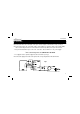
Schematic diagram 8. Schematic diagram.
PCB 9.
VELLEMAN Components NV Legen Heirweg 33 9890 Gavere Belgium Europe www.velleman.be www.velleman-kit.com Modifications and typographical errors reserved © Velleman Components nv.