nRF24L01 Single Chip 2.4GHz Transceiver Product Specification Key Features • • • • • • • • • • • • • • • • • • Worldwide 2.4GHz ISM band operation Up to 2Mbps on air data rate Ultra low power operation 11.3mA TX at 0dBm output power 12.3mA RX at 2Mbps air data rate 900nA in power down 22µA in standby-I On chip voltage regulator 1.9 to 3.
nRF24L01 Product Specification Liability disclaimer Nordic Semiconductor ASA reserves the right to make changes without further notice to the product to improve reliability, function or design. Nordic Semiconductor ASA does not assume any liability arising out of the application or use of any product or circuits described herein. All application information is advisory and does not form part of the specification.
nRF24L01 Product Specification Writing Conventions This product specification follows a set of typographic rules that makes the document consistent and easy to read. The following writing conventions are used: • Commands, bit state conditions, and register names are written in Courier. • Pin names and pin signal conditions are written in Courier bold. • Cross references are underlined and highlighted in blue. Revision History Date July 2007 Revision 2.0 Version 2.
nRF24L01 Product Specification Contents 1 1.1 1.2 2 2.1 2.2 3 4 5 5.1 5.2 5.3 5.4 5.5 5.6 5.7 6 6.1 6.1.1 6.1.2 6.1.3 6.1.4 6.1.5 6.1.6 6.1.7 6.2 6.3 6.4 6.5 6.6 7 7.1 7.2 7.3 7.3.1 7.3.2 7.3.3 7.3.4 7.3.5 7.4 7.4.1 7.4.2 7.4.3 7.4.4 7.5 Introduction ............................................................................................... Features ............................................................................................... Block diagram .............................................
nRF24L01 Product Specification 7.5.1 7.5.2 7.6 7.6.1 7.6.2 7.7 7.8 7.9 7.9.1 7.9.2 7.9.3 7.9.4 7.9.5 7.9.6 Auto Acknowledgement ................................................................... Auto Retransmission (ART) ............................................................. Enhanced ShockBurst flowcharts ........................................................ PTX operation.................................................................................. PRX operation .............................
nRF24L01 Product Specification Configuration ........................................................................................ Appendix D - Application example .......................................................... PCB layout examples ........................................................................... Appendix E - Stationary disturbance detection ..................................... Revision 2.
nRF24L01 Product Specification 1 Introduction The nRF24L01 is a single chip 2.4GHz transceiver with an embedded baseband protocol engine (Enhanced ShockBurst™), designed for ultra low power wireless applications. The nRF24L01 is designed for operation in the world wide ISM frequency band at 2.400 - 2.4835GHz. An MCU (microcontroller) and very few external passive components are needed to design a radio system with the nRF24L01.
nRF24L01 Product Specification 1.1 Features Features of the nRF24L01 include: • • • • • • • • Radio X Worldwide 2.4GHz ISM band operation X 126 RF channels X Common RX and TX pins X GFSK modulation X 1 and 2Mbps air data rate X 1MHz non-overlapping channel spacing at 1Mbps X 2MHz non-overlapping channel spacing at 2Mbps Transmitter X Programmable output power: 0, -6, -12 or -18dBm X 11.3mA at 0dBm output power Receiver X Integrated channel filters X 12.
nRF24L01 Product Specification 1.2 Block diagram RF Transmitter PA Baseband TX Filter CSN TX FIFOs GFSK Modulator SPI LNA ANT2 Radio Control VDD_PA DVDD Power Management IREF RF Synthesiser VSS XC2 RX FIFOs VDD XC1 GFSK Demodulator Figure 1. nRF24L01 block diagram Revision 2.
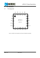
nRF24L01 Product Specification VDD VSS IREF Pin assignment DVDD 2.1 Pin Information VSS 2 20 19 18 17 16 CE 1 15 VDD CSN 2 14 VSS 13 ANT2 nRF24L01 SCK 3 QFN20 4X4 5 11 VDD_PA 6 7 8 9 10 XC1 MISO XC2 ANT1 VSS 12 VDD 4 IRQ MOSI Figure 2. nRF24L01 pin assignment (top view) for the QFN20 4x4 package Revision 2.
nRF24L01 Product Specification 2.
nRF24L01 Product Specification 3 Absolute maximum ratings Note: Exceeding one or more of the limiting values may cause permanent damage to nRF24L01. Operating conditions Supply voltages VDD VSS Input voltage VI Output voltage VO Total Power Dissipation PD (TA=85°C) Temperatures Operating Temperature Storage Temperature Minimum Maximum Units -0.3 3.6 0 V V -0.3 5.25 V VSS to VDD VSS to VDD -40 -40 Table 2. Absolute maximum ratings Revision 2.
nRF24L01 Product Specification 4 Operating conditions Symbol Parameter (condition) VDD Supply voltage Supply voltage if input signals >3.6V VDD TEMP Operating Temperature Notes Table 3. Operating conditions Revision 2.0 Page 13 of 74 Min. 1.9 2.7 -40 Typ. 3.0 3.0 +27 Max. Units 3.6 V 3.
nRF24L01 Product Specification 5 Electrical specifications Conditions: VDD = +3V, VSS = 0V, TA = - 40ºC to + 85ºC 5.1 Power consumption Symbol IVDD_PD IVDD_ST1 IVDD_ST2 IVDD_SU IVDD_TX0 IVDD_TX6 IVDD_TX12 IVDD_TX18 IVDD_AVG IVDD_TXS IVDD_2M IVDD_LC IVDD_1M IVDD_LC IVDD_RXS a. b. c. d. e. Parameter (condition) Notes Idle modes Supply current in power down a Supply current in standby-I mode Supply current in standby-II mode Average current during 1.
nRF24L01 Product Specification 5.2 General RF conditions Symbol fOP PLLres fXTAL Δf1M Δf2M RGFSK FCHAN- Parameter (condition) Operating frequency PLL Programming resolution Crystal frequency Frequency deviation @ 1Mbps Frequency deviation @ 2Mbps Air Data rate Non-overlapping channel spacNEL 1M ing @ 1Mbps FCHAN- Non-overlapping channel spacNEL 2M ing @ 2Mbps Notes Min. 2400 c 1 Units MHz MHz MHz kHz kHz kbps MHz c 2 MHz a Typ. Max. 2525 1 16 ±160 ±320 1000 b 2000 a.
nRF24L01 Product Specification 5.4 Receiver operation Symbol RXmax RXSENS RXSENS Parameter (condition) Maximum received signal at <0.1% BER Sensitivity (0.1%BER) @2Mbps Sensitivity at (0.1%BER) @1Mbps Notes Min. RX selectivity according to ETSI EN 300 440-1 V1.3.
nRF24L01 Product Specification 5.5 Crystal specifications Symbol Fxo ΔF C0 CL ESR Parameter (condition) Crystal Frequency Tolerance Equivalent parallel capacitance Load capacitance Equivalent Series Resistance Notes Min. ab 8 Typ. 16 ±60 1.5 12 Max. 7.0 16 100 a. Frequency accuracy including; tolerance at 25ºC, temperature drift, aging and crystal loading. b. Frequency regulations in certain regions sets tighter requirements to frequency tolerance (Ex: Japan and Korea max. +/- 50ppm) Table 8.
nRF24L01 Product Specification 5.6 DC characteristics Symbol VIH VIL Parameter (condition) HIGH level input voltage LOW level input voltage Notes Min. 0.7VDD VSS Typ. Max. Units V 5.25a 0.3VDD V a. If the input signal >3.6V, the VDD of the nRF24L01 must be between 2.7V and 3.3V (3.0V±10%) Table 9. Digital input pin Symbol VOH VOL Parameter (condition) HIGH level output voltage (IOH=-0.25mA) LOW level output voltage (IOL=0.25mA) Notes Min. VDD -0.3 Typ. Max. VDD 0.3 Units V V Max. 100 10.
nRF24L01 Product Specification 6 Radio Control This chapter describes the different modes the nRF24L01 radio transceiver can operate in and the parameters used to control the radio. The nRF24L01 has a built-in state machine that controls the transitions between the different operating modes of the chip. The state machine takes input from user defined register values and internal signals. 6.1 Operational Modes The nRF24L01 can be configured in four main modes of operation.
nRF24L01 Product Specification . Legend: Undefined Undefined Undefined VDD >= 1.9V Recommended operating mode Power on reset 10.3ms Possible operating mode Transition state Recommended path between operating modes Start up 1.
nRF24L01 Product Specification The register values are maintained during standby modes and the SPI may be activated. For start up time see Table 13. on page 22. 6.1.4 RX mode The RX mode is an active mode where the nRF24L01 radio is a receiver. To enter this mode, the nRF24L01 must have the PWR_UP bit set high, PRIM_RX bit set high and the CE pin set high. In this mode the receiver demodulates the signals from the RF channel, constantly presenting the demodulated data to the baseband protocol engine.
nRF24L01 Product Specification a. In this operating mode if the CE is held high the TX FIFO is emptied and all necessary ACK and possible retransmits are carried out. The transmission continues as long as the TX FIFO is refilled. If the TX FIFO is empty when the CE is still high, nRF24L01 enters standby-II mode. In this mode the transmission of a packet is started as soon as the CSN is set high after a upload (UL) of a packet to TX FIFO. b. This operating mode pulses the CE high for at least 10µs.
nRF24L01 Product Specification 6.3 RF channel frequency The RF channel frequency determines the center of the channel used by the nRF24L01. The channel occupies a bandwidth of 1MHz at 1Mbps and 2MHz at 2Mbps. nRF24L01 can operate on frequencies from 2.400GHz to 2.525GHz. The resolution of the RF channel frequency setting is 1MHz. At 2Mbps the channel occupies a bandwidth wider than the resolution of the RF channel frequency setting.
nRF24L01 Product Specification 7 Enhanced ShockBurst™ Enhanced ShockBurst™ is a packet based data link layer. It features automatic packet assembly and timing, automatic acknowledgement and re-transmissions of packets. Enhanced ShockBurst™ enables the implementation of ultra low power, high performance communication with low cost host microcontrollers.
nRF24L01 Product Specification 7.3 Enhanced Shockburst™ packet format The format of the Enhanced ShockBurst™ packet is described in this chapter. The Enhanched ShockBurst™ packet contains a preamble field, address field, packet control field, payload field and a CRC field. Figure 4. on page 25 shows the packet format with MSB to the left. P re a m b le 1 b y te A d d re s s 3 -5 b y te P a c k e t C o n tro l F ie ld 9 b it P a y lo a d 0 - 3 2 b y te C R C 1 -2 b y te Figure 4.
nRF24L01 Product Specification Coding: 000000 = 0 byte (only used in empty ACK packets.) 100000 = 32 byte, 100001 = Don’t care. This field is only used if the Dynamic Payload Length function is enabled. 7.3.3.2 PID (Packet identification) The 2 bit PID field is used to detect if the received packet is new or retransmitted. PID prevents the PRX device from presenting the same payload more than once to the MCU. The PID field is incremented at the TX side for each new packet received through the SPI.
nRF24L01 Product Specification With DPL feature the nRF24L01 can decode the payload length of the received packet automatically instead of using the RX_PW_Px registers. The MCU can read the length of the received payload by using the R_RX_PL_WID command. In order to enable DPL the EN_DPL bit in the FEATURE register must be set. In RX mode the DYNPD register has to be set. A PTX that transmits to a PRX with DPL enabled must have the DPL_P0 bit in DYNPD set. 7.4.
nRF24L01 Product Specification With static packet length the Enhanced ShockBurst™ will capture the packet according to the length given by the RX_PW register. With DPL Enhanced ShockBurst™ captures the packet according to the payload lenght field in the packet control field. After capturing the packet Enhanced ShockBurst™ will perform CRC. If the CRC is valid, Enhanced ShockBurst™ will check PID. The received PID is compared with the previous received PID.
nRF24L01 Product Specification 7.5.1 Auto Acknowledgement Auto acknowledgment is a function that automatically transmits an ACK packet to the PTX after it has received and validated a packet. The auto acknowledgement function reduces the load of the system MCU and can remove the need for dedicated SPI hardware. This also reduces cost and average current consumption. The Auto Acknowledgement feature is enabled by setting the EN_AA register.
nRF24L01 Product Specification nRF24L01 enters standby-I mode if there is no more untransmitted data in the TX FIFO and the CE pin is low. If the ACK packet is not received, nRF24L01 goes back to TX mode after a delay defined by ARD and retransmits the data. This continues until acknowledgment is received, or the maximum number of retransmits is reached. Set PWR_UP =0 to abort auto retransmission.
nRF24L01 Product Specification 7.6 Enhanced ShockBurst flowcharts This section shows flowcharts for PTX and PRX operation in Enhanced ShockBurst™. ShockBurst™ operation is marked with a dashed square in the flow charts. 7.6.1 PTX operation The flowchart in Figure 8. shows how a nRF24L01 configured as a PTX behaves after entering standby-I mode.
nRF24L01 Product Specification checks if the NO_ACK flag is set. If it is not set, the nRF24L01 enters RX mode to receive an ACK packet. If the received ACK packet is empty, only the TX_DS IRQ is asserted. If the ACK packet contains a payload, both TX_DS IRQ and RX_DR IRQ are asserted simultaneously before nRF24L01 returns to standby-I mode. If the ACK packet is not received before timeout occurs, the nRF24L01 returns to standby-I mode. It stays in standby-I mode until the ARD has elapsed.
nRF24L01 Product Specification 7.6.2 PRX operation The flowchart in Figure 9. shows how a nRF24L01 configured as a PRX behaves after entering standby-I mode.
nRF24L01 Product Specification with payload. If the No_ACK flag is not set in the received packet, the PRX enters TX mode. If there is a pending payload in the TX FIFO it is attached to the ACK packet. After the ACK packet is transmitted, the nRF24L01 returns to RX mode. A copy of a previously received packet might be received if the ACK packet is lost. In this case, the PRX discards the received packet and transmits an ACK packet before it returns to RX mode. Revision 2.
nRF24L01 Product Specification 7.7 Multiceiver Multiceiver is a feature used in RX mode that contains a set of 6 parallel data pipes with unique addresses. A data pipe is a logical channel in the physical RF channel. Each data pipe has its own physical address decoding in the nRF24L01. PTX3 PTX4 PTX2 2 Da ta P 5 Pi pe PTX6 Da ta Pipe 3 pe Pi Data Data ta Da PTX1 Pipe 4 PTX5 ipe 1 Da ip ta P e0 PRX Frequency Channel N Figure 10.
nRF24L01 Product Specification Note: Always ensure that none of the data pipes have the same address. Each pipe can have up to 5 byte configurable address. Data pipe 0 has a unique 5 byte address. Data pipes 1-5 share the 4 most significant address bytes. The LSByte must be unique for all 6 pipes. Figure 11. is an example of how data pipes 0-5 are addressed.
nRF24L01 Product Specification A3 B6 3 B5 B4 5B6A B3 0x 3B4B B 0x R: DD _P0: _A TX ADDR _ RX PTX3 TX RX _AD _A DR DD : R_ P0 0x :0 B3 xB B4 3B B5 4B B6 5B 0F 60 F The PRX, using multiceiver and Enhanced ShockBurst™, receives packets from more than one PTX. To ensure that the ACK packet from the PRX is transmitted to the correct PTX, the PRX takes the data pipe address where it received the packet and uses it as the TX address when transmitting the ACK packet. Figure 12.
nRF24L01 Product Specification 7.8 Enhanced ShockBurstTM timing This section describes the timing sequence of Enhanced ShockBurst™ and how all modes are initiated and operated. The Enhanced ShockBurst™ timing is controlled through the Data and Control interface. The nRF24L01 can be set to static modes or autonomous modes where the internal state machine controls the events. Each autonomous mode/sequence is ended with an interrupt at the IRQ pin.
nRF24L01 Product Specification TESB Cycle >10us TUL 130us TIRQ TOA IRQ: TX DS UL PTX SPI PTX CE PTX IRQ PTX MODE PRX MODE Standby 1 Standby 1 PLL Lock PLL Lock TX RX PLL Lock RX Standby 1 PLL Lock TX PLL Lock TACK 130us RX PRX IRQ PRX CE PRX SPI IRQ:RX DR/DL 130us 130us TIRQ Figure 14. Timing of Enhanced ShockBurst™ for one packet upload (2Mbps) In Figure 14. the transmission and acknowledgement of a packet are shown.
nRF24L01 Product Specification 7.9 Enhanced ShockBurstTM transaction diagram This section describes how several scenarios for the Enhanced ShockBurst™ automatic transaction handling. The call outs in this section’s figures indicate the IRQs and other events. For MCU activity the event may be placed at a different timeframe. Note: The figures in this section indicate the earliest possible download (DL) of the packet to the MCU and the latest possible upload (UL) of payload to the transmitter. 7.9.
nRF24L01 Product Specification 7.9.2 Single transaction with a lost packet Figure 16. is a scenario where a retransmission is needed due to loss of the first packet transmit. After the packet is transmitted, the PTX enters RX mode to receive the ACK packet. After the first transmission, the PTX waits a specified time for the ACK packet, if it is not in the specific time slot the PTX retransmits the packet as shown in Figure 16. MCU PTX UL IRQ Packet PID=1 lost during transmission No address detected.
nRF24L01 Product Specification 7.9.4 Single transaction with ACK payload packet Figure 18. is a scenario of the basic auto acknowledgement with payload. After the packet is transmitted by the PTX and received by the PRX the ACK packet with payload is transmitted from the PRX to the PTX. The RX_DR IRQ is asserted after the packet is received by the PRX, whereas on the PTX side the TX_DS IRQ is asserted when the ACK packet is received by the PTX.
nRF24L01 Product Specification 7.9.6 Two transactions with ACK payload packet and the first ACK packet lost. MCU PTX UL1 UL2 No address detected.
nRF24L01 Product Specification 7.10 Compatibility with ShockBurst™ The nRF24L01 can have the Enhanced ShockBurst™ feature disabled in order to be backward compatible with the nRF2401A, nRF24E1, nRF2402 and nRF24E2. Disabling the Enhanced ShockBurst™ features is done by setting register EN_AA=0x00 and the ARC = 0. In addition, the nRF24L01 air data rate must be set to 1Mbps. 7.10.1 ShockBurst™ packet format The ShockBurst™ packet format is described in this chapter. MSB to the left.
nRF24L01 Product Specification 8 Data and Control Interface The data and control interface gives you access to all the features in the nRF24L01.
nRF24L01 Product Specification Command name R_REGISTER W_REGISTER Command # Data bytes word (binary) 000A AAAA 1 to 5 LSByte first 001A AAAA 1 to 5 LSByte first R_RX_PAYLOAD 0110 0001 1 to 32 LSByte first W_TX_PAYLOAD 1010 0000 FLUSH_TX FLUSH_RX 1110 0001 1110 0010 1 to 32 LSByte first 0 0 REUSE_TX_PL 1110 0011 0 ACTIVATE 0101 0000 1 R_RX_PL_WIDa 0110 0000 W_ACK_PAYLOADa 1010 1PPP Revision 2.0 1 to 32 LSByte first Operation Read command and status registers.
nRF24L01 Product Specification Command # Data bytes Operation word (binary) 1011 000 1 to 32 Used in TX mode. Disables AUTOACK on this W_TX_PAYLOAD_NO a specific packet. LSByte first ACK NOP 1111 1111 0 No Operation. Might be used to read the STATUS register Command name a. To activate this feature use the ACTIVATE SPI command followed by data 0x73. The corresponding bits in the FEATURE register shown in Table 24. on page 58 have to be set. Table 16.
nRF24L01 Product Specification CSN SCK MOSI C7 C6 C5 C4 C3 C2 C1 C0 MISO S7 S6 S5 S4 S3 S2 S1 S0 D7 D6 D5 D4 D3 D2 D1 D0 D1 5 D1 4 D1 3 Figure 24. SPI write operation Tcwh CSN Tcc Tch Tcl Tcch SCK Tdh Tdc MOSI C7 C6 Tcsd MISO C0 Tcd Tcdz S7 S0 Figure 25. SPI NOP timing diagram Figure 26. shows the Rpull and Cload that are referenced in Table 18. to Table 23. Vdd Rpull Pin of nRF24L01 External Cload Figure 26. Rpull and Cload Revision 2.
nRF24L01 Product Specification Symbol Tdc Tdh Tcsd Tcd Tcl Tch Fsck Tr,Tf Tcc Tcch Tcwh Tcdz Parameters Data to SCK Setup SCK to Data Hold CSN to Data Valid SCK to Data Valid SCK Low Time SCK High Time SCK Frequency SCK Rise and Fall CSN to SCK Setup SCK to CSN Hold CSN Inactive time CSN to Output High Z Min 2 2 Max 38 55 40 40 0 8 100 2 2 50 38 Units ns ns ns ns ns ns MHz ns ns ns ns ns Table 18.
nRF24L01 Product Specification Symbol Tdc Tdh Tcsd Tcd Tcl Tch Fsck Tr,Tf Tcc Tcch Tcwh Tcdz Parameters Data to SCK Setup SCK to Data Hold CSN to Data Valid SCK to Data Valid SCK Low Time SCK High Time SCK Frequency SCK Rise and Fall CSN to SCK Setup SCK to CSN Hold CSN Inactive time CSN to Output High Z Min 2 2 Max 116 123 40 40 0 4 100 2 2 50 116 Units ns ns ns ns ns ns MHz ns ns ns ns ns Table 21.
nRF24L01 Product Specification 8.4 Data FIFO The data FIFOs are used to store payload that is transmitted (TX FIFO) or payload that is received and ready to be clocked out (RX FIFO). The FIFOs are accessible in both PTX mode and PRX mode. The following FIFOs are present in nRF24L01: • • TX three level, 32 byte FIFO RX three level, 32 byte FIFO Both FIFOs have a controller and are accessible through the SPI by using dedicated SPI commands.
nRF24L01 Product Specification 8.5 Interrupt The nRF24L01 has an active low interrupt (IRQ) pin. The IRQ pin is activated when TX_DS IRQ, RX_DR IRQ or MAX_RT IRQ are set high by the state machine in the STATUS register. The IRQ pin resets when MCU writes '1' to the IRQ source bit in the STATUS register. The IRQ mask in the CONFIG register is used to select the IRQ sources that are allowed to assert the IRQ pin. By setting one of the MASK bits high, the corresponding IRQ source is disabled.
nRF24L01 Product Specification 9 Register Map You can configure and control the radio chip by accessing the register map through the SPI by using read and write commands. 9.1 Register map table All undefined bits in the table below are redundant. They are read out as '0'. Note: Addresses 18 to 1B are reserved for test purposes, altering them will make the chip malfunction. Address (Hex) 00 01 02 Revision 2.
nRF24L01 Product Specification Address (Hex) 03 04 05 06 Revision 2.0 Mnemonic Bit ERX_P3 ERX_P2 ERX_P1 ERX_P0 3 2 1 0 Reset Value 0 0 1 1 SETUP_AW Reserved AW 7:2 1:0 000000 11 SETUP_RETR ARD 7:4 0000 ARC 3:0 0011 RF_CH Reserved RF_CH 7 6:0 0 0000010 RF_SETUP Reserved PLL_LOCK RF_DR 7:5 4 3 000 0 1 RF_PWR 2:1 11 LNA_HCURR 0 1 Type R/W R/W R/W R/W Description Enable data pipe 3. Enable data pipe 2. Enable data pipe 1. Enable data pipe 0.
nRF24L01 Product Specification Address (Hex) 07 Mnemonic Bit Reset Value Type STATUS Reserved RX_DR 7 6 0 0 R/W R/W TX_DS 5 0 R/W MAX_RT 4 0 R/W RX_P_NO 3:1 111 R TX_FULL 0 0 R OBSERVE_TX PLOS_CNT 7:4 0 R ARC_CNT 3:0 0 R CD Reserved CD 7:1 0 000000 0 R R 0A RX_ADDR_P0 39:0 0xE7E7E 7E7E7 0B RX_ADDR_P1 39:0 0xC2C2C 2C2C2 0C RX_ADDR_P2 7:0 0xC3 0D RX_ADDR_P3 7:0 0xC4 0E RX_ADDR_P4 7:0 0xC5 0F RX_ADDR_P5 7:0 0xC6 08 09 Revision 2.
nRF24L01 Product Specification Address (Hex) Mnemonic Bit 10 TX_ADDR 39:0 0xE7E7E 7E7E7 R/W Transmit address. Used for a PTX device only. (LSByte is written first) Set RX_ADDR_P0 equal to this address to handle automatic acknowledge if this is a PTX device with Enhanced ShockBurst™ enabled. See page 65. 11 RX_PW_P0 Reserved RX_PW_P0 7:6 5:0 00 0 R/W Only '00' allowed R/W Number of bytes in RX payload in data pipe 0 (1 to 32 bytes).
nRF24L01 Product Specification Address (Hex) Mnemonic Bit RX_PW_P4 5:0 Reset Value 0 RX_PW_P5 Reserved RX_PW_P5 7:6 5:0 00 0 FIFO_STATUS Reserved TX_REUSE 7 6 0 0 TX_FULL 5 0 TX_EMPTY 4 1 Reserved RX_FULL 3:2 1 00 0 RX_EMPTY 0 1 N/A ACK_PLDc 255:0 X N/A TX_PLD 255:0 X 16 17 Revision 2.0 Type Description R/W Number of bytes in RX payload in data pipe 4 (1 to 32 bytes).
nRF24L01 Product Specification Address (Hex) N/A 1C 1D Mnemonic Bit RX_PLD 255:0 Reset Value X Type R DYNPDc Reserved DPL_P5 7:6 5 0 0 R/W R/W DPL_P4 4 0 R/W DPL_P3 3 0 R/W DPL_P2 2 0 R/W DPL_P1 1 0 R/W DPL_P0 0 0 R/W 0 0 0 0 R/W R/W R/W R/W R/W FEATUREc Reserved EN_DPL EN_ACK_PAYd EN_DYN_ACK 7:3 2 1 0 Description Read by separate SPI command RX data payload register. 1 - 32 bytes. This register is implemented as a FIFO with three levels.
nRF24L01 Product Specification 10 Peripheral RF Information This chapter describes peripheral circuitry and PCB layout requirements that are important for achieving optimum RF performance from the nRF24L01. 10.1 Antenna output The ANT1 and ANT2 output pins provide a balanced RF output to the antenna. The pins must have a DC path to VDD_PA, either through a RF choke or through the center point in a balanced dipole antenna. A load of 15Ω+j88Ω is recommended for maximum output power (0dBm).
nRF24L01 Product Specification XO_OUT Buffer: Sine to full swing Amplitude controlled current source Current starved inverter: XOSC core Vdd Vdd Vss Vss ESD ESD XC1 XC2 Figure 28. Principle of crystal oscillator The nRF24L01 crystal oscillator is amplitude regulated. It is recommended to use an input signal larger than 0.4V-peak to achieve low current consumption and good signal-to-noise ratio when using an external clock. XC2 is not used and can be left as an open pin when clocked externally.
nRF24L01 Product Specification 11 Mechanical specifications nRF24L01 uses the QFN20 4x4 package, with matt tin plating. Revision 2.
nRF24L01 Product Specification Package Type Saw QFN20 (4x4 mm) Min Typ. Max A 0.80 0.85 0.95 A1 A3 K D/E e 0.00 0.02 0.20 0.20 min 4.0 0.5 BSC 0.05 REF. BSCa D2/E2 2.50 2.60 2.70 a. BSC: Basic Spacing between Centers, ref. JEDEC standard 95, page 4.17-11/A Figure 29. nRF24L01 Package Outline Revision 2.0 Page 62 of 74 L 0.35 0.40 0.45 L1 0.15 max b 0.18 0.25 0.
nRF24L01 Product Specification 12 Ordering information Ordering code nRF24L01-REEL nRF24L01-REEL7 nRF24L01 nRF24L01-EVKIT Description Package Container 2/1Mbps Transceiver 20 pin QFN 4x4 Tape and reelb 2/1Mbps Transceiver 20 pin QFN 4x4 Tape and reel 2/1Mbps Transceiver 20 pin QFN 4x4 Tray 2 node evaluation N/A N/A MOQa 4000 1500 490 1 a. MOQ = Minimum order quantity b. Moisture Sensitivity Level: MSL2@260ºC, three times reflow 12.1 n 2 Y Package marking R F B 4 L 0 1 Y W W L 12.
nRF24L01 Product Specification 13 Glossary of Terms Term ACK ART CE CLK CRC CSN ESB GFSK IRQ ISM LNA LSB LSByte Mbps MCU MISO MOSI MSB MSByte PCB PID PLD PRX PTX PWR_DWN PWR_UP RoHS RX RX_DR SPI TX TX_DS Description Acknowledgement Auto Re-Transmit Chip Enable Clock Cyclic Redundancy Check Chip Select NOT Enhanced ShockBurst™ Gaussian Frequency Shift Keying Interrupt Request Industrial-Scientific-Medical Low Noise Amplifier Least Significant Bit Least Significant Byte Megabit per second Microcontroller Un
nRF24L01 Product Specification Appendix A - Enhanced ShockBurst™ - Configuration and Communication Example Enhanced ShockBurst™ Transmitting Payload 1. 2. 3. 4. 5. 6. 7. The configuration bit PRIM_RX has to be low. When the application MCU has data to transmit, the address for the receiving node (TX_ADDR) and payload data (TX_PLD) has to be clocked into nRF24L01 through the SPI. The width of TXpayload is counted from number of bytes written into the TX FIFO from the MCU.
nRF24L01 Product Specification 5. 6. 7. 8. when RX_DR is high. RX_P_NO in STATUS register indicates what data pipe the payload has been received in. If auto acknowledgement is enabled, an ACK packet is transmitted back, unless the NO_ACK bit is set in the received packet. If there is a payload in the TX_PLD FIFO, this payload is added to the ACK packet. MCU sets the CE pin low to enter standby-I mode (low current mode). MCU can clock out the payload data at a suitable rate through the SPI.
nRF24L01 Product Specification Appendix B - Configuration for compatibility with nRF24XX How to setup nRF24L01 to receive from an nRF2401/nRF2402/nRF24E1/nRF24E2: 1. 2. 3. 4. 5. 6. 7. 8.
nRF24L01 Product Specification Appendix C - Carrier wave output power The output power of a radio is a critical factor for achieving wanted range. Output power is also the first test criteria needed to qualify for all telecommunication regulations. Configuration 1. 2. 3. 4. 5. 6. 7. 8. 9. 10. 11. 12. 13. 14. 15. Set PWR_UP = 1 in the CONFIG register Wait 1.
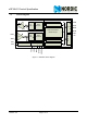
nRF24L01 Product Specification Appendix D - Application example nRF24L01 with single ended matching network crystal, bias resistor, and decoupling capacitors. C7 33nF 0402 C8 1nF 0402 1 2 3 4 5 CE CSN SCK MOSI MISO nRF24L01 15 14 13 12 11 VDD VSS ANT2 ANT1 VDD_PA C5 L3 L1 8.2nH 0402 IRQ VDD VSS XC2 XC1 CE CSN SCK MOSI MISO U1 VSS DVDD VDD VSS IREF C9 10nF 0402 R2 22K 0402 20 19 18 17 16 VDD 50ohm, RF I/O 3.9nH 0402 1.5pF 0402 C6 1.0pF 0402 L2 2.7nH 0402 6 7 8 9 10 NRF24L01 IRQ C3 2.
nRF24L01 Product Specification PCB layout examples Figure 31. on page 70, Figure 32. on page 71 and Figure 33. on page 71 show a PCB layout example for the application schematic in Figure 30. on page 69. A double-sided FR-4 board of 1.6mm thickness is used. This PCB has a ground plane on the bottom layer. Additionally, there are ground areas on the component side of the board to ensure sufficient grounding of critical components.
nRF24L01 Product Specification Figure 32. Top layer (nRF24L01 RF layout with single ended connection to PCB antenna and 0402 size passive components) Figure 33. Bottom layer (nRF24L01 RF layout with single ended connection to PCB antenna and 0402 size passive components The nest figure (Figure 34. on page 72, Figure 35. on page 72 and Figure 36. on page 73) is for the SMA output to have a board for direct measurements at a 50Ω SMA connector. Revision 2.
nRF24L01 Product Specification Figure 34. Top Overlay (Module with OFM crystal and SMA connector) Figure 35. Top Layer (Module with OFM crystal and SMA connector) Revision 2.
nRF24L01 Product Specification Figure 36. Bottom Layer (Module with OFM crystal and SMA connector) Revision 2.
nRF24L01 Product Specification Appendix E - Stationary disturbance detection In Enhanced ShockBurst™ it is recommended to use the Carrier Detect functionality only when the PTX device does not succeed to get packets through, as indicated by the MAX_RT IRQ for single packets and by the packet loss counter (PLOS_CNT) if several packets are lost.