
Data Sheet

Revision 2.0 Page 59 of 74
nRF24L01 Product Specification
10 Peripheral RF Information
This chapter describes peripheral circuitry and PCB layout requirements that are important for achieving
optimum RF performance from the nRF24L01.
10.1 Antenna output
The ANT1 and ANT2 output pins provide a balanced RF output to the antenna. The pins must have a DC
path to VDD_PA, either through a RF choke or through the center point in a balanced dipole antenna. A
load of 15Ω+j88Ω is recommended for maximum output power (0dBm). Lower load impedance (for
instance 50Ω) can be obtained by fitting a simple matching network between the load and ANT1 and ANT2.
A recommended matching network for 50
Ω load impedance is described in Appendix D on page 69.
10.2 Crystal oscillator
A crystal being used with the nRF24L01 must fulfil the specifications given in Table 8. on page 17.
To achieve a crystal oscillator solution with low power consumption and fast start-up time a crystal with a
low load capacitance specification must be used. A lower C
0
also gives lower current consumption and
faster start-up time, but may increase the cost of the crystal. Typically C
0
=1.5pF at a crystal specified for
C
0max
=7.0pF.
The crystal load capacitance, C
L, is given by:
, where C
1
’ = C
1
+ C
PCB1
+C
I1
and C
2
’ = C
2
+ C
PCB2
+ C
I2
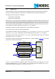
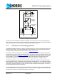
C1 and C2 are SMD capacitors as shown in the application schematics, see Figure 30. on page 69. CPCB1
and CPCB2 are the layout parasitic on the circuit board. CI1 and CI2 are the capacitance seen into the XC1
and XC2 pins respectively; the value is typically 1pF for each of these pins.
10.3 nRF24L01 sharing crystal with an MCU
When using an MCU to drive the crystal reference input XC1 of the nRF24L01 transceiver the rules
described in the following sections (10.3.1
and 10.3.2) must be followed.
10.3.1 Crystal parameters
The requirement of load capacitance C
L
is only set by the MCU when the MCU drives the nRF24L01 clock
input. The frequency accuracy of ±60ppm is still required to get a functional radio link. The nRF24L01
loads the crystal by 1pF in addition to the PCB routing.
10.3.2 Input crystal amplitude and current consumption
The input signal should not have amplitudes exceeding any rail voltage. Exceeding rail voltage excites the
ESD structure and the radio performance is degraded below specification. You must use an external DC
block if you are testing the nRF24L01 with a reference source that has no DC offset (which is often the
case with a RF source).
''
''
21
21
CC
CC
L
C
+
⋅
=