MFRC522 Standard performance MIFARE and NTAG frontend Rev. 3.9 — 27 April 2016 112139 Product data sheet COMPANY PUBLIC 1. Introduction This document describes the functionality and electrical specifications of the contactless reader/writer MFRC522. Remark: The MFRC522 supports all variants of the MIFARE Mini, MIFARE 1K, MIFARE 4K, MIFARE Ultralight, MIFARE DESFire EV1 and MIFARE Plus RF identification protocols.
MFRC522 NXP Semiconductors Standard performance MIFARE and NTAG frontend The following host interfaces are provided: • Serial Peripheral Interface (SPI) • Serial UART (similar to RS232 with voltage levels dependant on pin voltage supply) • I2C-bus interface 3.
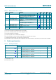
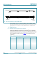
MFRC522 NXP Semiconductors Standard performance MIFARE and NTAG frontend Table 1. Quick reference data …continued Symbol Parameter Conditions Ipd power-down current VDDA = VDDD = VDD(TVDD) = VDD(PVDD) = 3 V Min Typ Max Unit hard power-down; pin NRSTPD set LOW [4] - - 5 A soft power-down; RF level detector on [4] - - 10 A IDDD digital supply current pin DVDD; VDDD = 3 V - 6.
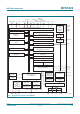
MFRC522 NXP Semiconductors Standard performance MIFARE and NTAG frontend 6. Block diagram The analog interface handles the modulation and demodulation of the analog signals. The contactless UART manages the protocol requirements for the communication protocols in cooperation with the host. The FIFO buffer ensures fast and convenient data transfer to and from the host and the contactless UART and vice versa. Various host interfaces are implemented to meet different customer requirements.
MFRC522 NXP Semiconductors Standard performance MIFARE and NTAG frontend D6/ADR_0/ D4/ADR_2 MOSI/MX D5/ADR_1/ D7/SCL/ D3/ADR_3 SCK/DTRQ MISO/TX D2/ADR_4 SDA/NSS/RX EA 24 I2C 32 D1/ADR_5 1 25 27 26 30 29 28 PVDD PVSS 2 31 5 3 VOLTAGE MONITOR AND POWER ON DETECT SPI, UART, I2C-BUS INTERFACE CONTROL 4 15 18 FIFO CONTROL DVDD DVSS AVDD AVSS STATE MACHINE 64-BYTE FIFO BUFFER COMMAND REGISTER RESET CONTROL PROGRAMABLE TIMER POWER-DOWN CONTROL CONTROL REGISTER BANK 6 23 INTERRUPT C
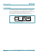
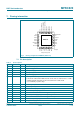
MFRC522 NXP Semiconductors Standard performance MIFARE and NTAG frontend 25 D1/ADR_5 26 D2/ADR_4 27 D3/ADR_3 28 D4/ADR_2 29 D5/ADR_1/SCK/DTRQ 30 D6/ADR_0/MOSI/MX 31 D7/SCL/MISO/TX 32 EA 7. Pinning information I2C 1 24 SDA/NSS/RX PVDD 2 23 IRQ DVDD 3 22 OSCOUT DVSS 4 PVSS 5 NRSTPD 6 19 AUX1 MFIN 7 18 AVSS MFOUT 8 17 RX 21 OSCIN VMID 16 20 AUX2 AVDD 15 TVSS 14 TX2 13 TVDD 12 TX1 11 9 SVDD TVSS 10 MFRC522 001aaj819 Transparent top view Fig 3.
MFRC522 NXP Semiconductors Standard performance MIFARE and NTAG frontend Table 3. Pin description …continued Pin Symbol Type[1] Description 16 VMID P internal reference voltage 17 RX I RF signal input 18 AVSS G analog ground 19 AUX1 O auxiliary outputs for test purposes 20 AUX2 O auxiliary outputs for test purposes 21 OSCIN I crystal oscillator inverting amplifier input; also the input for an externally generated clock (fclk = 27.
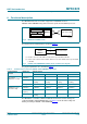
MFRC522 NXP Semiconductors Standard performance MIFARE and NTAG frontend 8. Functional description The MFRC522 transmission module supports the Read/Write mode for ISO/IEC 14443 A/MIFARE using various transfer speeds and modulation protocols. BATTERY MFRC522 ISO/IEC 14443 A CARD MICROCONTROLLER contactless card reader/writer Fig 4. 001aak583 MFRC522 Read/Write mode The physical level communication is shown in Figure 5.
MFRC522 NXP Semiconductors Standard performance MIFARE and NTAG frontend ISO/IEC 14443 A framing at 106 kBd start 8-bit data 8-bit data odd parity start bit is 1 8-bit data odd parity odd parity ISO/IEC 14443 A framing at 212 kBd, 424 kBd and 848 kBd start 8-bit data even parity 8-bit data odd parity start bit is 0 8-bit data odd parity burst of 32 subcarrier clocks even parity at the end of the frame 001aak585 Fig 6.
MFRC522 NXP Semiconductors Standard performance MIFARE and NTAG frontend 8.1.2 Serial Peripheral Interface A serial peripheral interface (SPI compatible) is supported to enable high-speed communication to the host. The interface can handle data speeds up to 10 Mbit/s. When communicating with a host, the MFRC522 acts as a slave, receiving data from the external host for register settings, sending and receiving data relevant for RF interface communication.
MFRC522 NXP Semiconductors Standard performance MIFARE and NTAG frontend 8.1.2.2 SPI write data To write data to the MFRC522 using SPI requires the byte order shown in Table 7. It is possible to write up to n data bytes by only sending one address byte. The first send byte defines both the mode and the address byte. Table 7. MOSI and MISO byte order Line Byte 0 Byte 1 Byte 2 MOSI address 0 data 0 MISO X[1] X[1] [1] To Byte n Byte n + 1 data 1 ... data n 1 data n X[1] ...
MFRC522 NXP Semiconductors Standard performance MIFARE and NTAG frontend 8.1.3.2 Selectable UART transfer speeds The internal UART interface is compatible with an RS232 serial interface. The default transfer speed is 9.6 kBd. To change the transfer speed, the host controller must write a value for the new transfer speed to the SerialSpeedReg register. Bits BR_T0[2:0] and BR_T1[4:0] define the factors for setting the transfer speed in the SerialSpeedReg register.
MFRC522 NXP Semiconductors Standard performance MIFARE and NTAG frontend 8.1.3.3 UART framing Table 11. UART framing Bit Length Value Start 1-bit 0 Data 8 bits data Stop 1-bit 1 Remark: The LSB for data and address bytes must be sent first. No parity bit is used during transmission. Read data: To read data using the UART interface, the flow shown in Table 12 must be used. The first byte sent defines both the mode and the address. Table 12.
MFRC522 NXP Semiconductors Standard performance MIFARE and NTAG frontend Table 13. MFRC522 Product data sheet COMPANY PUBLIC Write data byte order Pin Byte 0 Byte 1 RX (pin 24) address 0 data 0 TX (pin 31) - address 0 All information provided in this document is subject to legal disclaimers. Rev. 3.9 — 27 April 2016 112139 © NXP Semiconductors N.V. 2016. All rights reserved.
xxxxxxxxxxxxxxxxxxxxx xxxxxxxxxxxxxxxxxxxxxxxxxx xxxxxxx x x x xxxxxxxxxxxxxxxxxxxxxxxxxxxxxx xxxxxxxxxxxxxxxxxxx xx xx xxxxx xxxxxxxxxxxxxxxxxxxxxxxxxxx xxxxxxxxxxxxxxxxxxx xxxxxx xxxxxxxxxxxxxxxxxxxxxxxxxxxxxxxxxxx xxxxxxxxxxxx x x xxxxxxxxxxxxxxxxxxxxx xxxxxxxxxxxxxxxxxxxxxxxxxxxxxx xxxxx xxxxxxxxxxxxxxxxxxxxxxxxxxxxxxxxxxxxxxxxxxxxxxxxxx xxxxxxxx xxxxxxxxxxxxxxxxxxxxxxxxx xxxxxxxxxxxxxxxxxxxx xxx NXP Semiconductors MFRC522 Product data sheet COMPANY PUBLIC DATA ADDRESS RX SA A0 A1 A2 A3 A4 A5
MFRC522 NXP Semiconductors Standard performance MIFARE and NTAG frontend Table 14. Address byte 0 register; address MOSI 7 (MSB) 6 5 1 = read 0 = write reserved address 4 3 2 1 0 (LSB) 8.1.4 I2C-bus interface An I2C-bus (Inter-IC) interface is supported to enable a low-cost, low pin count serial bus interface to the host. The I2C-bus interface is implemented according to NXP Semiconductors’ I2C-bus interface specification, rev. 2.1, January 2000. The interface can only act in Slave mode.
MFRC522 NXP Semiconductors Standard performance MIFARE and NTAG frontend 8.1.4.1 Data validity Data on the SDA line must be stable during the HIGH clock period. The HIGH or LOW state of the data line must only change when the clock signal on SCL is LOW. SDA SCL data line stable; data valid change of data allowed mbc621 Fig 12. Bit transfer on the I2C-bus 8.1.4.2 START and STOP conditions To manage the data transfer on the I2C-bus, unique START (S) and STOP (P) conditions are defined.
MFRC522 NXP Semiconductors Standard performance MIFARE and NTAG frontend 8.1.4.4 Acknowledge An acknowledge must be sent at the end of one data byte. The acknowledge-related clock pulse is generated by the master. The transmitter of data, either master or slave, releases the SDA line (HIGH) during the acknowledge clock pulse. The receiver pulls down the SDA line during the acknowledge clock pulse so that it remains stable LOW during the HIGH period of this clock pulse.
MFRC522 NXP Semiconductors Standard performance MIFARE and NTAG frontend 8.1.4.5 7-Bit addressing During the I2C-bus address procedure, the first byte after the START condition is used to determine which slave will be selected by the master. Several address numbers are reserved. During device configuration, the designer must ensure that collisions with these reserved addresses cannot occur. Check the I2C-bus specification for a complete list of reserved addresses.
MFRC522 NXP Semiconductors Standard performance MIFARE and NTAG frontend 8.1.4.7 Register read access To read out data from a specific register address in the MFRC522, the host controller must use the following procedure: • Firstly, a write access to the specific register address must be performed as indicated in the frame that follows • The first byte of a frame indicates the device address according to the I2C-bus rules • The second byte indicates the register address.
MFRC522 NXP Semiconductors Standard performance MIFARE and NTAG frontend 8.1.4.8 High-speed mode In High-speed mode (HS mode), the device can transfer information at data rates of up to 3.4 Mbit/s, while remaining fully downward-compatible with Fast or Standard mode (F/S mode) for bidirectional communication in a mixed-speed bus system. 8.1.4.9 High-speed transfer To achieve data rates of up to 3.4 Mbit/s the following improvements have been made to I2C-bus operation.
MFRC522 NXP Semiconductors Standard performance MIFARE and NTAG frontend A 8-bit master code 0000 1xxx S t1 tH SDA high SCL high 1 2 to 5 6 7 8 9 F/S mode R/W 7-bit SLA Sr n + (8-bit data A + A/A) Sr P SDA high SCL high 1 2 to 5 6 7 8 9 1 2 to 5 6 7 8 9 If P then F/S mode HS mode If Sr (dotted lines) then HS mode tH tFS = Master current source pull-up msc618 = Resistor pull-up Fig 19.
MFRC522 NXP Semiconductors Standard performance MIFARE and NTAG frontend 8.1.4.11 Switching between F/S mode and HS mode After reset and initialization, the MFRC522 is in Fast mode (which is in effect F/S mode as Fast mode is downward-compatible with Standard mode). The connected MFRC522 recognizes the “S 00001XXX A” sequence and switches its internal circuitry from the Fast mode setting to the HS mode setting. The following actions are taken: 1.
MFRC522 NXP Semiconductors Standard performance MIFARE and NTAG frontend 8.2 Analog interface and contactless UART 8.2.1 General The integrated contactless UART supports the external host online with framing and error checking of the protocol requirements up to 848 kBd. An external circuit can be connected to the communication interface pins MFIN and MFOUT to modulate and demodulate the data.
MFRC522 NXP Semiconductors Standard performance MIFARE and NTAG frontend Table 16.
MFRC522 NXP Semiconductors Standard performance MIFARE and NTAG frontend 8.2.3 Serial data switch Two main blocks are implemented in the MFRC522. The digital block comprises the state machines, encoder/decoder logic. The analog block comprises the modulator and antenna drivers, the receiver and amplifiers. It is possible for the interface between these two blocks to be configured so that the interfacing signals are routed to pins MFIN and MFOUT.
MFRC522 NXP Semiconductors Standard performance MIFARE and NTAG frontend Remark: Pins MFIN and MFOUT have a dedicated supply on pin SVDD with the ground on pin PVSS. If pin MFIN is not used it must be connected to either pin SVDD or pin PVSS. If pin SVDD is not used it must be connected to either pin DVDD, pin PVDD or any other voltage supply pin. MFRC522 Product data sheet COMPANY PUBLIC All information provided in this document is subject to legal disclaimers. Rev. 3.
xxxxxxxxxxxxxxxxxxxxx xxxxxxxxxxxxxxxxxxxxxxxxxx xxxxxxx x x x xxxxxxxxxxxxxxxxxxxxxxxxxxxxxx xxxxxxxxxxxxxxxxxxx xx xx xxxxx xxxxxxxxxxxxxxxxxxxxxxxxxxx xxxxxxxxxxxxxxxxxxx xxxxxx xxxxxxxxxxxxxxxxxxxxxxxxxxxxxxxxxxx xxxxxxxxxxxx x x xxxxxxxxxxxxxxxxxxxxx xxxxxxxxxxxxxxxxxxxxxxxxxxxxxx xxxxx xxxxxxxxxxxxxxxxxxxxxxxxxxxxxxxxxxxxxxxxxxxxxxxxxx xxxxxxxx xxxxxxxxxxxxxxxxxxxxxxxxx xxxxxxxxxxxxxxxxxxxx xxx NXP Semiconductors MFRC522 Product data sheet COMPANY PUBLIC MFOUT TX bit stream DIGITAL MODULE MFRC5
MFRC522 NXP Semiconductors Standard performance MIFARE and NTAG frontend 8.2.5 CRC coprocessor The following CRC coprocessor parameters can be configured: • The CRC preset value can be either 0000h, 6363h, A671h or FFFFh depending on the ModeReg register’s CRCPreset[1:0] bits setting • The CRC polynomial for the 16-bit CRC is fixed to x16 + x12 + x5 + 1 • The CRCResultReg register indicates the result of the CRC calculation.
MFRC522 NXP Semiconductors Standard performance MIFARE and NTAG frontend • FIFO buffer almost empty warning: Status1Reg register’s LoAlert bit • FIFO buffer overflow warning: ErrorReg register’s BufferOvfl bit. The BufferOvfl bit can only be cleared by setting the FIFOLevelReg register’s FlushBuffer bit. The MFRC522 can generate an interrupt signal when: • ComIEnReg register’s LoAlertIEn bit is set to logic 1. It activates pin IRQ when Status1Reg register’s LoAlert bit changes to logic 1.
MFRC522 NXP Semiconductors Standard performance MIFARE and NTAG frontend The ComIrqReg register’s ErrIRq bit indicates an error detected by the contactless UART during send or receive. This is indicated when any bit is set to logic 1 in register ErrorReg. Table 18.
MFRC522 NXP Semiconductors Standard performance MIFARE and NTAG frontend The timer can be started manually using the ControlReg register’s TStartNow bit and stopped using the ControlReg register’s TStopNow bit. The timer can also be activated automatically to meet any dedicated protocol requirements by setting the TModeReg register’s TAuto bit to logic 1. The delay time of a timer stage is set by the reload value + 1.
MFRC522 NXP Semiconductors Standard performance MIFARE and NTAG frontend 8.6 Power reduction modes 8.6.1 Hard power-down Hard power-down is enabled when pin NRSTPD is LOW. This turns off all internal current sinks including the oscillator. All digital input buffers are separated from the input pins and clamped internally (except pin NRSTPD). The output pins are frozen at either a HIGH or LOW level. 8.6.
MFRC522 NXP Semiconductors Standard performance MIFARE and NTAG frontend The clock applied to the MFRC522 provides a time basis for the synchronous system’s encoder and decoder. The stability of the clock frequency, therefore, is an important factor for correct operation. To obtain optimum performance, clock jitter must be reduced as much as possible. This is best achieved using the internal oscillator buffer with the recommended circuitry.
MFRC522 NXP Semiconductors Standard performance MIFARE and NTAG frontend 9. MFRC522 registers 9.1 Register bit behavior Depending on the functionality of a register, the access conditions to the register can vary. In principle, bits with same behavior are grouped in common registers. The access conditions are described in Table 19. Table 19.
MFRC522 NXP Semiconductors Standard performance MIFARE and NTAG frontend 9.2 Register overview Table 20.
MFRC522 NXP Semiconductors Standard performance MIFARE and NTAG frontend Table 20.
MFRC522 NXP Semiconductors Standard performance MIFARE and NTAG frontend 9.3 Register descriptions 9.3.1 Page 0: Command and status 9.3.1.1 Reserved register 00h Functionality is reserved for future use. Table 21. Reserved register (address 00h); reset value: 00h bit allocation Bit 7 5 4 3 Symbol reserved Access - Table 22. 9.3.1.2 6 2 1 0 Reserved register bit descriptions Bit Symbol Description 7 to 0 - reserved CommandReg register Starts and stops command execution. Table 23.
MFRC522 NXP Semiconductors Standard performance MIFARE and NTAG frontend Table 26. 9.3.1.
MFRC522 NXP Semiconductors Standard performance MIFARE and NTAG frontend Table 30. ComIrqReg register bit descriptions All bits in the ComIrqReg register are cleared by software.
MFRC522 NXP Semiconductors Standard performance MIFARE and NTAG frontend 9.3.1.7 ErrorReg register Error bit register showing the error status of the last command executed. Table 33. ErrorReg register (address 06h); reset value: 00h bit allocation Bit 7 6 5 4 3 2 1 0 Symbol WrErr TempErr reserved BufferOvfl CollErr CRCErr ParityErr ProtocolErr Access R R - R R R R R Table 34.
MFRC522 NXP Semiconductors Standard performance MIFARE and NTAG frontend 9.3.1.8 Status1Reg register Contains status bits of the CRC, interrupt and FIFO buffer. Table 35. Status1Reg register (address 07h); reset value: 21h bit allocation Bit 7 Symbol 6 5 reserved CRCOk CRCReady Access Table 36.
MFRC522 NXP Semiconductors Standard performance MIFARE and NTAG frontend 9.3.1.9 Status2Reg register Contains status bits of the receiver, transmitter and data mode detector. Table 37. Status2Reg register (address 08h); reset value: 00h bit allocation Bit 7 6 Symbol TempSensClear I2CForceHS reserved MFCrypto1On ModemState[2:0] Access R/W R/W - D R Table 38.
MFRC522 NXP Semiconductors Standard performance MIFARE and NTAG frontend 9.3.1.10 FIFODataReg register Input and output of 64 byte FIFO buffer. Table 39. Bit FIFODataReg register (address 09h); reset value: xxh bit allocation 7 6 5 4 3 Symbol FIFOData[7:0] Access D 2 1 Table 40.
MFRC522 NXP Semiconductors Standard performance MIFARE and NTAG frontend Table 44.
MFRC522 NXP Semiconductors Standard performance MIFARE and NTAG frontend 9.3.1.14 BitFramingReg register Adjustments for bit-oriented frames. Table 47. Bit BitFramingReg register (address 0Dh); reset value: 00h bit allocation 7 6 5 4 3 2 1 0 Symbol StartSend RxAlign[2:0] reserved TxLastBits[2:0] Access W R/W - R/W Table 48.
MFRC522 NXP Semiconductors Standard performance MIFARE and NTAG frontend Table 50.
MFRC522 NXP Semiconductors Standard performance MIFARE and NTAG frontend 9.3.2.2 ModeReg register Defines general mode settings for transmitting and receiving. Table 55. Bit ModeReg register (address 11h); reset value: 3Fh bit allocation 7 Symbol 6 5 4 MSBFirst reserved TxWaitRF reserved Access R/W Table 56.
MFRC522 NXP Semiconductors Standard performance MIFARE and NTAG frontend Table 58. TxModeReg register bit descriptions Bit Symbol Value Description 7 TxCRCEn 1 enables CRC generation during data transmission Remark: can only be set to logic 0 at 106 kBd 6 to 4 TxSpeed[2:0] defines the bit rate during data transmission the MFRC522 handles transfer speeds up to 848 kBd 9.3.2.
MFRC522 NXP Semiconductors Standard performance MIFARE and NTAG frontend Table 60. RxModeReg register bit descriptions …continued Bit Symbol Value Description 2 RxMultiple 0 receiver is deactivated after receiving a data frame 1 able to receive more than one data frame only valid for data rates above 106 kBd in order to handle the polling command after setting this bit the Receive and Transceive commands will not terminate automatically.
MFRC522 NXP Semiconductors Standard performance MIFARE and NTAG frontend 9.3.2.6 TxASKReg register Controls transmit modulation settings. Table 63. Bit TxASKReg register (address 15h); reset value: 00h bit allocation 7 Symbol 6 4 3 reserved Force100ASK Access - Table 64. 2 1 0 reserved R/W - TxASKReg register bit descriptions Bit Symbol Value Description 7 reserved - 6 Force100ASK 1 5 to 0 reserved 9.3.2.
MFRC522 NXP Semiconductors Standard performance MIFARE and NTAG frontend Table 66. TxSelReg register bit descriptions …continued Bit Symbol 3 to 0 MFOutSel [3:0] 0000 Value Description selects the input for pin MFOUT 3-state 0001 9.3.2.
MFRC522 NXP Semiconductors Standard performance MIFARE and NTAG frontend 9.3.2.9 RxThresholdReg register Selects thresholds for the bit decoder. Table 69. RxThresholdReg register (address 18h); reset value: 84h bit allocation Bit 7 6 5 4 3 2 1 0 Symbol MinLevel[3:0] reserved CollLevel[2:0] Access R/W - R/W Table 70.
MFRC522 NXP Semiconductors Standard performance MIFARE and NTAG frontend Table 72. DemodReg register bit descriptions …continued Bit Symbol Value Description 4 TPrescalEven R/W Available on RC522 version 1.0 and version 2.0: If set to logic 0 the following formula is used to calculate the timer frequency of the prescaler: ftimer = 13.56 MHz / (2*TPreScaler+1). Only available on version 2.
MFRC522 NXP Semiconductors Standard performance MIFARE and NTAG frontend Table 77. Bit MfTxReg register (address 1Ch); reset value: 62h bit allocation 7 6 5 4 3 2 1 0 Symbol reserved TxWait[1:0] Access - R/W Table 78. MfTxReg register bit descriptions Bit Symbol Description 7 to 2 reserved reserved for future use 1 to 0 TxWait defines the additional response time 7 bits are added to the value of the register bit by default 9.3.2.14 MfRxReg register Table 79.
MFRC522 NXP Semiconductors Standard performance MIFARE and NTAG frontend MFRC522 Product data sheet COMPANY PUBLIC Table 84. SerialSpeedReg register bit descriptions Bit Symbol Description 7 to 5 BR_T0[2:0] factor BR_T0 adjusts the transfer speed: for description, see Section 8.1.3.2 on page 12 4 to 0 BR_T1[4:0] factor BR_T1 adjusts the transfer speed: for description, see Section 8.1.3.2 on page 12 All information provided in this document is subject to legal disclaimers. Rev. 3.
MFRC522 NXP Semiconductors Standard performance MIFARE and NTAG frontend 9.3.3 Page 2: Configuration 9.3.3.1 Reserved register 20h Functionality is reserved for future use. Table 85. Bit 9.3.3.2 Reserved register (address 20h); reset value: 00h bit allocation 7 6 5 4 3 Symbol - Access reserved Table 86. Reserved register bit descriptions Bit Symbol Description 7 to 0 reserved reserved for future use 2 1 0 CRCResultReg registers Shows the MSB and LSB values of the CRC calculation.
MFRC522 NXP Semiconductors Standard performance MIFARE and NTAG frontend 9.3.3.3 Reserved register 23h Functionality is reserved for future use. Table 91. Bit 9.3.3.4 Reserved register (address 23h); reset value: 88h bit allocation 7 6 5 4 3 Symbol reserved Access - Table 92. Reserved register bit descriptions Bit Symbol Description 7 to 0 reserved reserved for future use 2 1 0 ModWidthReg register Sets the modulation width. Table 93.
MFRC522 NXP Semiconductors Standard performance MIFARE and NTAG frontend 9.3.3.6 RFCfgReg register Configures the receiver gain. Table 97. Bit 7 6 5 4 3 2 1 Symbol reserved RxGain[2:0] reserved Access - R/W - Table 98. 0 RFCfgReg register bit descriptions Bit Symbol Value Description 7 reserved - reserved for future use 6 to 4 RxGain [2:0] 000 18 dB 001 23 dB 010 18 dB 011 23 dB 100 33 dB 101 38 dB 110 43 dB 111 48 dB 3 to 0 9.3.3.
MFRC522 NXP Semiconductors Standard performance MIFARE and NTAG frontend 9.3.3.8 CWGsPReg register Defines the conductance of the p-driver output during periods of no modulation. Table 101. CWGsPReg register (address 28h); reset value: 20h bit allocation Bit 7 6 5 4 3 2 Symbol reserved CWGsP[5:0] Access - R/W 1 0 Table 102.
MFRC522 NXP Semiconductors Standard performance MIFARE and NTAG frontend Table 106.
MFRC522 NXP Semiconductors Standard performance MIFARE and NTAG frontend Table 108. TPrescalerReg register bit descriptions Bit Symbol Description 7 to 0 TPrescaler_Lo[7:0] defines the lower 8 bits of the TPrescaler value The following formula is used to calculate the timer frequency if the DemodReg register’s TPrescalEven bit is set to logic 0: ftimer = 13.56 MHz / (2*TPreScaler+1).
MFRC522 NXP Semiconductors Standard performance MIFARE and NTAG frontend Table 113. TCounterValReg (higher bits) register (address 2Eh); reset value: xxh bit allocation Bit 7 6 5 4 3 Symbol TCounterVal_Hi[7:0] Access R 2 1 0 Table 114. TCounterValReg register higher bit descriptions Bit Symbol Description 7 to 0 TCounterVal_Hi [7:0] timer value higher 8 bits Table 115.
MFRC522 NXP Semiconductors Standard performance MIFARE and NTAG frontend Table 120. TestSel1Reg register bit descriptions 9.3.4.3 Bit Symbol Description 7 to 3 reserved reserved for future use 2 to 0 TstBusBitSel [2:0] selects a test bus signal which is output at pin MFOUT if AnalogSelAux2[3:0] = FFh in AnalogTestReg register, test bus signal is also output at pins AUX1 or AUX2 TestSel2Reg register General test signal configuration and PRBS control. Table 121.
MFRC522 NXP Semiconductors Standard performance MIFARE and NTAG frontend Table 124. TestPinEnReg register bit descriptions Bit Symbol Value Description 7 RS232LineEn 0 6 to 1 TestPinEn [5:0] serial UART lines MX and DTRQ are disabled - enables the output driver on one of the data pins D1 to D7 which outputs a test signal Example: setting bit 1 to logic 1 enables pin D1 output setting bit 5 to logic 1 enables pin D5 output Remark: If the SPI is used, only pins D1 to D4 can be used.
MFRC522 NXP Semiconductors Standard performance MIFARE and NTAG frontend Table 128. TestBusReg register bit descriptions Bit Symbol Description 7 to 0 TestBus[7:0] shows the status of the internal test bus the test bus is selected using the TestSel2Reg register; see Section 16.1 on page 82 9.3.4.7 AutoTestReg register Controls the digital self-test. Table 129.
MFRC522 NXP Semiconductors Standard performance MIFARE and NTAG frontend 9.3.4.9 AnalogTestReg register Determines the analog output test signal at, and status of, pins AUX1 and AUX2. Table 133. AnalogTestReg register (address 38h); reset value: 00h bit allocation Bit 7 6 5 4 3 2 1 Symbol AnalogSelAux1[3:0] AnalogSelAux2[3:0] Access R/W R/W 0 Table 134.
MFRC522 NXP Semiconductors Standard performance MIFARE and NTAG frontend 9.3.4.10 TestDAC1Reg register Defines the test value for TestDAC1. Table 135. TestDAC1Reg register (address 39h); reset value: xxh bit allocation Bit 7 6 5 4 3 2 Symbol reserved TestDAC1[5:0] Access - R/W 1 0 Table 136.
MFRC522 NXP Semiconductors Standard performance MIFARE and NTAG frontend Table 141. Reserved register (address 3Ch); reset value: FFh bit allocation Bit 7 6 5 4 3 Symbol RFT Access - 2 1 0 1 0 1 0 1 0 Table 142. Reserved register bit descriptions Bit Symbol Description 7 to 0 reserved reserved for production tests Table 143. Reserved register (address 3Dh); reset value: 00h bit allocation Bit 7 6 5 4 3 Symbol RFT Access - 2 Table 144.
MFRC522 NXP Semiconductors Standard performance MIFARE and NTAG frontend 10. MFRC522 command set 10.1 General description The MFRC522 operation is determined by a state machine capable of performing a set of commands. A command is executed by writing a command code (see Table 149) to the CommandReg register. Arguments and/or data necessary to process a command are exchanged via the FIFO buffer. 10.
MFRC522 NXP Semiconductors Standard performance MIFARE and NTAG frontend 10.3.1 MFRC522 command descriptions 10.3.1.1 Idle Places the MFRC522 in Idle mode. The Idle command also terminates itself. 10.3.1.2 Mem Transfers 25 bytes from the FIFO buffer to the internal buffer. To read out the 25 bytes from the internal buffer the Mem command must be started with an empty FIFO buffer. In this case, the 25 bytes are transferred from the internal buffer to the FIFO.
MFRC522 NXP Semiconductors Standard performance MIFARE and NTAG frontend 10.3.1.7 Receive The MFRC522 activates the receiver path and waits for a data stream to be received. The correct settings must be chosen before starting this command. This command automatically terminates when the data stream ends. This is indicated either by the end of frame pattern or by the length byte depending on the selected frame type and speed.
MFRC522 NXP Semiconductors Standard performance MIFARE and NTAG frontend This command automatically terminates when the MIFARE card is authenticated and the Status2Reg register’s MFCrypto1On bit is set to logic 1. This command does not terminate automatically if the card does not answer, so the timer must be initialized to automatic mode. In this case, in addition to the IdleIRq bit, the TimerIRq bit can be used as the termination criteria.
MFRC522 NXP Semiconductors Standard performance MIFARE and NTAG frontend 11. Limiting values Table 150. Limiting values In accordance with the Absolute Maximum Rating System (IEC 60134). Symbol Parameter VDDA VDDD Conditions Min Max Unit analog supply voltage 0.5 +4.0 V digital supply voltage 0.5 +4.0 V VDD(PVDD) PVDD supply voltage 0.5 +4.0 V VDD(TVDD) TVDD supply voltage 0.5 +4.0 V VDD(SVDD) SVDD supply voltage 0.5 +4.
MFRC522 NXP Semiconductors Standard performance MIFARE and NTAG frontend 13. Thermal characteristics Table 152. Thermal characteristics Symbol Parameter Rth(j-a) thermal resistance from junction to ambient Conditions Package Typ in still air with exposed pin soldered on a 4 layer JEDEC PCB HVQFN32 40 Unit K/W 14. Characteristics Table 153.
MFRC522 NXP Semiconductors Standard performance MIFARE and NTAG frontend Table 153. Characteristics …continued Symbol Parameter Conditions Min Typ Max Unit Ci input capacitance VDDA = 2.8 V; DC = 0.65 V; AC = 1 V (p-p) - 2 - pF - +1 A Input/output characteristics pins D1, D2, D3, D4, D5, D6 and D7 ILI input leakage current 1 VIH HIGH-level input voltage 0.7VDD(PVDD) - - V VIL LOW-level input voltage - - 0.
MFRC522 NXP Semiconductors Standard performance MIFARE and NTAG frontend Table 153. Characteristics …continued Symbol Parameter Conditions Min Typ Max Unit VOH HIGH-level output voltage VDD(TVDD) = 3 V; IDD(TVDD) = 32 mA; CWGsP[5:0] = 3Fh VDD(TVDD) 0.15 - - V VDD(TVDD) = 3 V; IDD(TVDD) = 80 mA; CWGsP[5:0] = 3Fh VDD(TVDD) 0.4 - - V VDD(TVDD) = 2.5 V; IDD(TVDD) = 32 mA; CWGsP[5:0] = 3Fh VDD(TVDD) 0.24 - - V VDD(TVDD) = 2.5 V; IDD(TVDD) = 80 mA; CWGsP[5:0] = 3Fh VDD(TVDD) 0.
MFRC522 NXP Semiconductors Standard performance MIFARE and NTAG frontend Table 153. Characteristics …continued Symbol Parameter Conditions Min Typ Max Unit VOH HIGH-level output voltage pin OSCOUT - 1.1 - V VOL LOW-level output voltage pin OSCOUT - 0.2 - V Ci input capacitance pin OSCOUT - 2 - pF pin OSCIN - 2 - pF Typical input requirements fxtal crystal frequency - 27.
MFRC522 NXP Semiconductors Standard performance MIFARE and NTAG frontend Table 154. SPI timing characteristics …continued Symbol Parameter Conditions Min Typ Max Unit tsu(D-SCKH) data input to SCK HIGH set-up time changing MOSI to SCK 25 - - ns th(SCKL-Q) SCK LOW to data output hold time SCK to changing MISO - - 25 ns 0 - - ns 50 - - ns t(SCKL-NSSH) SCK LOW to NSS HIGH time tNHNL NSS high before communication Table 155.
MFRC522 NXP Semiconductors Standard performance MIFARE and NTAG frontend tSCKL tSCKH tSCKL SCK tSLDX tDXSH tSHDX tDXSH MOSI MSB LSB MISO MSB LSB tSLNH NSS 001aaj634 Remark: The signal NSS must be LOW to be able to send several bytes in one data stream. To send more than one data stream NSS must be set HIGH between the data streams. Fig 25. Timing diagram for SPI SDA tSU;DAT tf tSP tr tHD;STA tf tLOW tBUF SCL tr tHD;STA S tHIGH tHD;DAT tSU;STA tSU;STO Sr P S 001aaj635 Fig 26.
MFRC522 NXP Semiconductors Standard performance MIFARE and NTAG frontend 15. Application information A typical application diagram using a complementary antenna connection to the MFRC522 is shown in Figure 27. The antenna tuning and RF part matching is described in the application note Ref. 1 and Ref. 2.
MFRC522 NXP Semiconductors Standard performance MIFARE and NTAG frontend 16. Test information 16.1 Test signals 16.1.1 Self test The MFRC522 has the capability to perform a digital self test. The self test is started by using the following procedure: 1. Perform a soft reset. 2. Clear the internal buffer by writing 25 bytes of 00h and implement the Config command. 3. Enable the self test by writing 09h to the AutoTestReg register. 4. Write 00h to the FIFO buffer. 5.
MFRC522 NXP Semiconductors Standard performance MIFARE and NTAG frontend Table 156. Test bus signals: TestBusSel[4:0] = 07h Pins Internal signal name Description D6 s_data received data stream D5 s_coll bit-collision detected (106 kBd only) D4 s_valid s_data and s_coll signals are valid D3 s_over receiver has detected a stop condition D2 RCV_reset receiver is reset D1 - reserved Table 157.
MFRC522 NXP Semiconductors Standard performance MIFARE and NTAG frontend Table 158. Test signal descriptions …continued 16.1.3.1 AnalogSelAux1[3:0] or AnalogSelAux2[3:0] value Signal on pin AUX1 or pin AUX2 1101 RxActive 1110 subcarrier detected 1111 TstBusBit Example: Output test signals TestDAC1 and TestDAC2 The AnalogTestReg register is set to 11h. The output on pin AUX1 has the test signal TestDAC1 and the output on pin AUX2 has the test signal TestDAC2.
MFRC522 NXP Semiconductors Standard performance MIFARE and NTAG frontend 001aak598 (1) (2) (3) 10 μs/div (1) MinLevel (1 V/div) on pin AUX2. (2) Corr1 (1 V/div) on pin AUX1. (3) RF field. Fig 29. Output test signals Corr1 on pin AUX1 and MinLevel on pin AUX2 16.1.3.3 Example: Output test signals ADC channel I and ADC channel Q Figure 30 shows the channel behavior test signals ADC_I and ADC_Q on pins AUX1 and AUX2, respectively. The AnalogTestReg register is set to 56h.
MFRC522 NXP Semiconductors Standard performance MIFARE and NTAG frontend 16.1.3.4 Example: Output test signals RxActive and TxActive Figure 31 shows the RxActive and TxActive test signals relating to RF communication. The AnalogTestReg register is set to CDh. • At 106 kBd, RxActive is HIGH during data bits, parity and CRC reception.
MFRC522 NXP Semiconductors Standard performance MIFARE and NTAG frontend 16.1.3.5 Example: Output test signal RX data stream Figure 32 shows the data stream that is currently being received. The TestSel2Reg register’s TestBusSel[4:0] bits are set to 07h to enable test bus signals on pins D1 to D6; see Section 16.1.2 on page 82.
MFRC522 NXP Semiconductors Standard performance MIFARE and NTAG frontend 17. Package outline HVQFN32: plastic thermal enhanced very thin quad flat package; no leads; 32 terminals; body 5 x 5 x 0.85 mm A B D SOT617-1 terminal 1 index area A A1 E c detail X C e1 e 1/2 e b 9 y y1 C v M C A B w M C 16 L 17 8 e e2 Eh 1/2 1 terminal 1 index area e 24 32 25 X Dh 0 2.5 5 mm scale DIMENSIONS (mm are the original dimensions) UNIT A(1) max.
MFRC522 NXP Semiconductors Standard performance MIFARE and NTAG frontend Detailed package information can be found at: http://www.nxp.com/package/SOT617-1.html. 18. Handling information Moisture Sensitivity Level (MSL) evaluation has been performed according to SNW-FQ-225B rev.04/07/07 (JEDEC J-STD-020C). MSL for this package is level 1 which means 260 C convection reflow temperature. Dry pack is not required. Unlimited out-of-pack floor life at maximum ambient 30 C/85 % RH. 19.
MFRC522 NXP Semiconductors Standard performance MIFARE and NTAG frontend 20. Abbreviations Table 159.
MFRC522 NXP Semiconductors Standard performance MIFARE and NTAG frontend 22. Revision history Table 160. Revision history Document ID Release date Data sheet status Change notice Supersedes MFRC522 v.3.9 20160427 Product data sheet - MFRC522 v.3.8 Modifications: MFRC522 v.3.8 Modifications: MFRC522 v.3.7 Modifications: MFRC522 v.3.
MFRC522 NXP Semiconductors Standard performance MIFARE and NTAG frontend 23. Legal information 23.1 Data sheet status Document status[1][2] Product status[3] Definition Objective [short] data sheet Development This document contains data from the objective specification for product development. Preliminary [short] data sheet Qualification This document contains data from the preliminary specification. Product [short] data sheet Production This document contains the product specification.
MFRC522 NXP Semiconductors Standard performance MIFARE and NTAG frontend Export control — This document as well as the item(s) described herein may be subject to export control regulations. Export might require a prior authorization from competent authorities. Quick reference data — The Quick reference data is an extract of the product data given in the Limiting values and Characteristics sections of this document, and as such is not complete, exhaustive or legally binding.
MFRC522 NXP Semiconductors Standard performance MIFARE and NTAG frontend 25. Contents 1 Introduction . . . . . . . . . . . . . . . . . . . . . . . . . . . . 1 2 General description . . . . . . . . . . . . . . . . . . . . . . 1 2.1 Differences between version 1.0 and 2.0 . . . . . 1 3 Features and benefits . . . . . . . . . . . . . . . . . . . . 2 4 Quick reference data . . . . . . . . . . . . . . . . . . . . . 2 5 Ordering information . . . . . . . . . . . . . . . . . . . . . 3 6 Block diagram . . . . .
MFRC522 NXP Semiconductors Standard performance MIFARE and NTAG frontend 9.3.3.2 CRCResultReg registers . . . . . . . . . . . . . . . . 9.3.3.3 Reserved register 23h . . . . . . . . . . . . . . . . . . 9.3.3.4 ModWidthReg register . . . . . . . . . . . . . . . . . . 9.3.3.5 Reserved register 25h . . . . . . . . . . . . . . . . . . 9.3.3.6 RFCfgReg register . . . . . . . . . . . . . . . . . . . . . 9.3.3.7 GsNReg register . . . . . . . . . . . . . . . . . . . . . . . 9.3.3.8 CWGsPReg register . . . . . .