TB6560AHQ/AFG TOSHIBA BiCD Integrated Circuit Silicon Monolithic TB6560AHQ, TB6560AFG PWM Chopper-Type Bipolar Driver IC for Stepping Motor Control The TB6560AHQ/AFG is a PWM chopper-type stepping motor driver IC designed for sinusoidal-input microstep control of bipolar stepping motors. The TB6560AHQ/AFG can be used in applications that require 2-phase, 1-2-phase, 2W1-2-phase and 4W1-2-phase excitation modes.
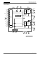
TB6560AHQ/AFG Block Diagram VDD Protect 20/30, 31 19/28 VMA MO 17/23 18/25, 26 OUT_AP M1 23/36 16/19, 20 PWM control circuit M2 22/35 Bridge driver A 13/10, 11 OUT_AM CW/CCW 21/33 CLK 3/45 RESET 5/48 ENABLE 4/47 Thermal shutdown circuit Input circuit 14/13, 14 NFA 8/55, 56 VMB DCY1 25/39 PWM control circuit DCY2 24/38 OUT_BP 12/6, 7 Bridge driver B 9/61, 62 OSC 7/53 OUT_BM OSC 11/2, 4 NFB Maximum current setting circuit 2/43 1/42 TQ1 TQ2 6/50, 51 15/16 SGND PGNDA 10/6
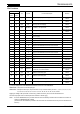
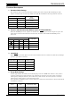
TB6560AHQ/AFG Pin Functions Pin No.
TB6560AHQ/AFG Equivalent Circuits Input Pins (M1, M2, CLK, CW/CCW, TQ1,TQ2,ENABLE, RESET ,DCY1, DCY2) Output Pins (MO, Protect) VDD 100 Ω 100 kΩ 100 Ω 4 2014-10-01
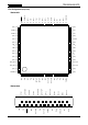
TB6560AHQ/AFG Pin Assignment (top view) (NC) RESET ENABLE (NC) CLK (NC) TQ1 TQ2 (NC) (NC) DCY1 DCY2 (NC) M1 M2 (NC) CW/CCW TB6560AFG 48 47 46 45 44 43 42 41 40 39 38 37 36 35 34 33 49 32 (NC) SGND 50 31 VDD SGND 51 30 VDD (NC) 52 29 (NC) 24 (NC) (NC) 58 23 MO (NC) 59 22 (NC) (NC) 60 21 (NC) OUT_BM 61 20 OUT_AP OUT_BM 62 19 OUT_AP (NC) 63 18 (NC) PGNDB 64 17 (NC) 4 5 6 7 8 9 10 11 OUT_AM 3 OUT_BP 2 NFB 1 12 13 14 15 16
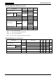
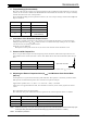
TB6560AHQ/AFG Absolute Maximum Ratings (Ta = 25°C) Characteristics Power supply voltage Output current (per phase) TB6560AHQ Peak TB6560AFG Rating VDD 6 VMA/B 40 Unit V 3.5 IO (PEAK) MO drain current Protect drain current Symbol A 2.5 I (MO) 1 mA I (Protect) 1 mA VIN VDD V Input voltage 5 (Note 1) TB6560AHQ Power dissipation 43 (Note 2) PD 1.7 (Note 3) TB6560AFG W 4.
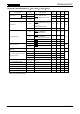
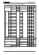
TB6560AHQ/AFG Electrical Characteristics (Ta = 25°C, VDD = 5 V, VM = 24 V) Characteristics Input voltage Symbol VDD −0.2 0.8 400 IIN (H) M1, M2, CW/CCW, CLK, RESET , ENABLE, DCY1, DCY2, TQ1, TQ2 VIN = 5.
TB6560AHQ/AFG Electrical Characteristics (Ta = 25°C, VDD = 5 V, VM = 24 V) Characteristics Symbol TB6560AHQ Output ON-resistance TB6560AFG A-/B-phase chopping current (Note 1) 2W1-2phase excitation 4W1-2phase excitation Test Condition Ron U1H Min Typ. Max 0.3 0.4 0.3 0.4 0.35 0.5 0.35 0.5 θ=0 100 IOUT = 1.5 A Ron L1H Ron U1F IOUT = 1.
TB6560AHQ/AFG Functional Descriptions 1. Excitation Mode Settings The excitation mode can be selected from the following four modes using the M1 and M2 inputs. (The 2-phase excitation mode is selected by default since both M1 and M2 have internal pull-down resistors.) Inputs M2 M1 Mode (Excitation) L L 2-phase L H 1-2-phase H L 4W1-2-phase H H 2W1-2-phase 2. Function Table (Relationship Between Inputs and Output Modes) When the ENABLE pin is Low, outputs are off.
TB6560AHQ/AFG 5. Torque Settings (Current Value) The ratio of the current necessary for actual operations to the predefined current adjusted by an external resistor can be selected as follows. The Weak Excitation mode should be selected to set a torque extremely low like when the motor is at a fixed position. Since the TQ2 and TQ1 pins have pull-down resistors, the 100 % torque setting is selected when TQ2 and TQ1 are undriven.
TB6560AHQ/AFG Relationship between the Enable and RESET and Output Signals Example 1: ENABLE input in 1-2-phase excitation mode (M1: H, M2: L) CW CLK ENABLE RESET MO voltage (%) 100 71 IA (current from 0 OUT_AP to OUT_AM) −71 −100 t0 t1 t2 t3 OFF t7 t8 t9 t10 t11 t12 Setting the ENABLE signal Low disables only the output signals, while internal circuitry other than the output block continues to operate in accordance with the CLK input.
TB6560AHQ/AFG 2-Phase Excitation (M1: L, M2: L, CW Mode) CW CLK MO (%) 100 IA 0 −100 (%) 100 IB 0 −100 t0 t1 t2 t3 t4 t5 t6 t7 1-2-Phase Excitation (M1: H, M2: L, CW Mode) CW CLK MO (%) 100 71 IA 0 −71 −100 (%) 100 71 IB 0 −71 −100 t0 t1 t2 t3 t4 t5 t6 12 t7 t8 2014-10-01
TB6560AHQ/AFG 2W1-2-Phase Excitation (M1: H, M2: H, CW Mode) CW CLK MO (%) 100 98 92 83 71 56 38 20 IA 0 −20 −38 −56 −71 −83 −92 −98 −100 (%) 100 98 92 83 71 56 38 IB 20 0 −20 −38 −56 −71 −83 −92 −98 −100 t0 t1 t2 t3 t4 t5 t6 t7 t8 t9 t10 t11 t12 t13 t14 t15 t16 t17 t18 t19 t20 t21 t22 t23 t24 t25 t26 t27 t28 t29 t30 t31 t32 13 2014-10-01
TB6560AHQ/AFG 4W1-2-Phase Excitation (M1: L, M2: H, CW Mode) [%] 100 98 96 92 88 83 77 71 63 56 47 38 29 A-phase B-phase 20 10 0 −10 −20 −29 −38 −47 −56 −63 −71 −77 −83 −88 −92 −96 −98 −100 STEP 14 2014-10-01
TB6560AHQ/AFG CK MO M1 M2 RESET (%) 100 91 71.4 40 IA 0 −40 −71.4 −91 −100 1-2-phase excitation Other excitation It is recommended that the state of the M1 and M2 pins be changed after setting the RESET signal Low during the Initial state (MO = Low). Even when the MO signal is Low, changing the M1 and M2 signals without setting the RESET signal Low may cause a discontinuity in the current waveform.
TB6560AHQ/AFG 9. Current Waveforms and Mixed Decay Mode Settings The current decay rate of the Decay mode operation can be determined by the DCY1 and DCY2 inputs for constant-current control. The “NF” refers to the point at which the output current reaches its predefined current level, and the “RNF” refers to the monitoring timing of the predefined current. The smaller the MDT value, the smaller the current ripple amplitude. However, the current decay rate decreases.
TB6560AHQ/AFG 10. Current Control Modes (Effects of Decay Modes) • Increasing the current (sine wave) Slow Slow Predefined Current Level Fast Predefined Current Level • Slow Charge Slow Fast Charge Charge Fast Charge Fast Decreasing the current with a high decay rate (The current decay rate in Mixed Decay mode is the ratio between the time in Fast-Decay mode (discharge time after MDT) and the remainder of the period.
TB6560AHQ/AFG 11.
TB6560AHQ/AFG 12. Current Waveform in Fast Decay Mode After the output current to the load reaches the current value specified by RNF, torque or other means, the output current to the load will be fed back to the power supply fully in Fast Decay mode.
TB6560AHQ/AFG 13. CLK and Internal OSC Signals and Output Current Waveform (when the CLK signal is asserted during Slow Decay mode) 25 % Mixed Decay Mode fchop fchop fchop OSC Pin Internal Waveform Predefined Current Level NF MDT IOUT NF Predefined Current Level RNF MDT RNF Switches to Charge mode briefly CLK Signal Input The OSC counter is reset here. When the CLK signal is asserted, the Chopping Counter (OSC Counter) is forced to reset at the next rising edge of the OSC signal.
TB6560AHQ/AFG 14. CLK and Internal OSC Signals and Output Current Waveform (when the CLK signal is asserted during Charge mode) 25 % Mixed Decay Mode fchop fchop fchop OSC Pin Internal Waveform Predefined Current Level MDT NF Predefined Current Level MDT IOUT RNF RNF Switches to Charge mode briefly CLK Signal Input The OSC Counter is reset here.
TB6560AHQ/AFG 15. CLK and Internal OSC Signals and Output Current Waveform (when the CLK signal is asserted during Fast Decay mode) 25 % Mixed Decay Mode fchop fchop fchop OSC Pin Internal Waveform Predefined Current Level IOUT NF MDT NF Predefined Current Level MDT RNF RNF Switches to Charge mode briefly CLK Signal Input The OSC Counter is reset here.
TB6560AHQ/AFG 16. Internal OSC Signal and Output Current Waveform when Predefined Current is Changed from Positive to Negative (when the CLK signal is input using 2-phase excitation) 25% Mixed Decay Mode fchop fchop fchop Predefined Current Level IOUT 0 RNF RNF Predefined Current Level NF MDT NF CLK Signal Input The OSC Counter is reset here.
TB6560AHQ/AFG Current Discharge Path when ENABLE is Set as Low During Operation When all the output transistors are forced off during Slow Decay mode, the coil energy is discharged in the following modes: Note: Parasitic diodes are located on dotted lines. However, they are not normally used in normal Mixed Decay mode.
TB6560AHQ/AFG Output Transistor Operating Modes VM VM U1 U2 U1 OFF OFF OFF ON ON L1 L2 L1 ON Note VM Note Load Load U2 U1 OFF OFF L2 ON RNF L1 Load L2 OFF RNF PGND Charge Mode ON Note ON RNF PGND U2 PGND Slow Mode Fast Mode Output Transistor Operating Modes CLK U1 U2 L1 L2 Charge ON OFF OFF ON Slow Decay OFF OFF ON ON Fast Decay OFF ON ON OFF Note: This table shows an example of when the current flows as indicated by the arrows in the above figures.
TB6560AHQ/AFG Test Points for AC Specifications CLK tCLK tCLK tpLH VM 90% 90% tpHL 50% 50% 10% GND 10% tr Figure 1 tf Timing Waveforms and Symbols OSC-Charge DELAY: The OSC waveform is converted into the internal OSC waveform by checking the level of a chopping wave. The internal OSC signal is designed to be logic High when the OSC voltage is at 2 V or above, and to be logic Low when the OSC voltage is at 0.5 V or below.
TB6560AHQ/AFG Power Dissipation TB6560AHQ TB6560AFG Power dissipation PD (W) PD - Ta ①With soldered leads.
TB6560AHQ/AFG 1. Power-on Sequence with Control Input Signals Turn on VDD. Then, when the VDD voltage has stabilized, turn on VMA/B. Hold the control input pins Low while turning on VDD and VMA/B. (All the control input pins are internally pulled down.) After VDD and VMA/B completely stabilizes at the rated voltages, the RESET and ENABLE pins can be set High. If this sequence is not properly followed, the IC may not operate correctly, or the IC and the peripheral parts may be damaged.
TB6560AHQ/AFG Application Circuit Example Fuse 5 V 10 µF 1 µF VDD CLK VMA 24 V VMB OUT_AP RESET ENABLE 1 µF 47 µF H-SW A OUT_AM Logic PWM control circuit M1 NFCompA M2 OUT_BP M H-SW B MCU or External input CW/CCW DCY1 OUT_BM Current control NFA PWM control circuit DCY2 RNFA NFCompB TQ1 TQ2 NFB Protect MO R1 R2 RNFB OSC 100 pF ≈ 400 kHz SGND PGND 0.5 Ω: IOUT (max) = 1.0 A Note: Capacitors for the power supply lines should be connected as close to the IC as possible.
TB6560AHQ/AFG Package Dimensions Weight: 9.86 g (typ.
TB6560AHQ/AFG Package Dimensions Weight: 0.26 g (typ.) Note: The size of a backside heatsink is 5.5 mm × 5.5 mm.
TB6560AHQ/AFG Notes on Contents 1. Block Diagrams Some of the functional blocks, circuits, or constants in the block diagram may be omitted or simplified for explanatory purposes. 2. Equivalent Circuits The equivalent circuit diagrams may be simplified or some parts of them may be omitted for explanatory purposes. 3. Timing Charts Timing charts may be simplified for explanatory purposes. 4. Application Circuits The application circuits shown in this document are provided for reference purposes only.
TB6560AHQ/AFG Points to Remember on Handling of ICs (1) Thermal Shutdown Circuit Thermal shutdown circuits do not necessarily protect ICs under all circumstances. If the thermal shutdown circuits operate against the over temperature, clear the heat generation status immediately. Depending on the method of use and usage conditions, such as exceeding absolute maximum ratings can cause the thermal shutdown circuit to not operate properly or IC breakdown before operation.
TB6560AHQ/AFG RESTRICTIONS ON PRODUCT USE • Toshiba Corporation, and its subsidiaries and affiliates (collectively "TOSHIBA"), reserve the right to make changes to the information in this document, and related hardware, software and systems (collectively "Product") without notice. • This document and any information herein may not be reproduced without prior written permission from TOSHIBA.