
Data Sheet

TB6560AHQ/AFG
2014-10-01
25
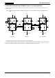
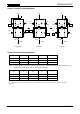
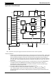
Output Transistor Operating Modes
Output Transistor Operating Modes
CLK U1 U2 L1 L2
Charge ON OFF OFF ON
Slow Decay OFF OFF ON ON
Fast Decay OFF ON ON OFF
Note: This table shows an example of when the current flows as indicated by the arrows in the above figures. If the
current flows in the opposite direction, refer to the following table:
CLK U1 U2 L1 L2
Charge OFF ON ON OFF
Slow Decay OFF OFF ON ON
Fast Decay ON OFF OFF ON
Upon transitions of above-mentioned modes, a dead time of about 300 ns is inserted between each mode
respectively.
U1
L1
U2
L2
PGND
OFF
OFF
U1
L1
U2
L2
OFF
ON
Note
Load
PGND
U1
L1
U2
L2
Note
Load
PGND
Note
R
NF
VM
ON
ON
Load
Charge Mode
Slow Mode
Fast Mode
ON
R
NF
VM
R
NF
VM
OFF
OFF
OFF
ON
ON