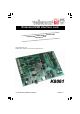
Extended USB interface card al US 3I/O univers 3 l fu e s u y ll A practica ard.
Features & specifications This interface board has a total of 33 input/outputs: including analogue / digital and + 1PWM output. Connection to the computer is galvanically-optically isolated, so that damage to the computer is not possible thus providing a high level of secure implementation. All communication routines are contained in a Dynamic Link Library (DLL). You may write custom Windows*.
Assembly hints 1. Assembly (Skipping this can lead to troubles ! ) Ok, so we have your attention. These hints will help you to make this project successful. Read them carefully. 1.1 Make sure you have the right tools: • A good quality soldering iron (25-40W) with a small tip. • Wipe it often on a wet sponge or cloth, to keep it clean; then apply solder to the tip, to give it a wet look. This is called ‘thinning’ and will protect the tip, and enables you to make good connections.
Assembly hints 1.
Construction 1. Jumpers J1 J2 J3 J4 J5 2. Diodes. Watch the polarity! D... CATHODE D1 : 1N4007 D2 : 1N4148 D3 : 1N4148 3. 1/4W Resistors R... R1 : 2K2 R2 : 15E R3 : 15E (2 - 2 - 2 - B) (1 - 5 - 0 - B) (1 - 5 - 0 - B) 4. Metal film resistors R... R4 : 100E (1 - 0 - 1 - B - 9) 5. 1/4W Resistors R...
Construction 6. Zenerdiode. Watch the polarity! ZD... CATHODE ZD1 : 15V0 7. Resistor array. ! RA1 RA2 RA3 RA4 9. IC sockets. Watch the position of the notch! IC1 IC2 IC3 IC4 IC5 IC6 : : : : : : 8p 8p 28p 18p 18p 40p IC7 : IC8 : IC9 : IC10 : IC11 : 10. LEDs. Watch the polarity! : : : : 1K 10K 1K 10K (102) (103) (102) (103) LD... CATHODE Watch the position of the dot. 8. Ceramic Capacitors C ...
Construction 15. Electrolytic capacitor. Watch the polarity! 12. Pin headers C3 : 470µF / 25V C... 16. DC-jack A1 A2 A3 AD1 AD2 AD3 AD4 AD5 AD6 AD7 AD8 DA1 DA2 DA3 DA4 DA5 DA6 DA7 DA8 J... + SK2 : 12VDC SW - Card adress 17. USB connector SK1 Analog inputs 18. Voltage regulator VR1 : UA7805 Analog outputs VR... 13. Electrolytic capacitors. Watch the polarity! C9 : 4,7µF / 50V C10 : 47µF / 25V 19. Shunts C... C15 : 4,7µF / 50V C16 : 4,7µF / 50V 20. Board to wire connectors 14.
Construction 22. Rubber feet 21. IC's. Watch the position of the notch! Mount the rubber feet on the solder side of the PCB, see fig 1.0. IC1 : 6N136 IC2 : 6N136 IC3 : VK8061USB (programmed PIC18F2550-I/SP) IC4 : ULN2803 IC5 : ULN2803 IC6 : VK8061CPU (programmed PIC16F871-I/P) IC7 : TLC5628CN IC8 : IC9 : IC10 : IC11 : TLV274IN TLV274IN TLV274IN TLV274IN FIG 1.0 23.
connection points 1 USB-connector 2 12VDC 3 4 Digital inputs 1, 2, 3, 4 Digital inputs 5, 6, 7, 8 Connection of the K8061 with the USB port of your PC Power supply connection. Connect a 12V non-regulated adapter supplying min. 300mA Inputs need to go “LOW” externally to activate (connect with the GND). These outputs are open collector outputs. When active, the transistors in IC4 will conduct and a “connection” will be established between GND and the output in question.
software installation 24. Software installation After assembly of the circuit, it is now time to install the software drivers and examples and to test the K8061. Connect a 12V power supply (non regulated 12V adapter) to the power supply connector of the K8061 (SK2). The control LED LD12 (RUN) should light as well as LD13 to LD20 (these are the input control LEDs and light when the inputs are not active “LOW”). If OK, connect the USB connector of the K8061 to your PC using the included USB cable.
software installation Step 3 : Browse through the driver folder on your hard disk or included CD. Select driver : mchpusb.
software installation Installation is successful A utility to check the operation of the K8061 can be found in the “DIAG8061” subfolder. A more elaborate test application can be found in the “DEMO8061” subfolder. The source code of the test application can be found in the “DLL examples” subfolder. Explanation concerning the communication DLL of the K8061 can be found in the “DOC” subfolder.
Connection example 25. How to connect : 2. Analog input : 1. Analog output : GND ! ANALOG OUTPUT VOLTAGE MAX 10V DC ! DAx : + GND 0 till 5V 0 ... 5V or 0 ... 10V OR 0 till 10V 3. Digital output : ADx : + 4. Digital input : +V Switch, ... +V :External power supply for relay, LED, Lamp.
Schematic diagram 26.
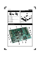
PCB 27. PCB layout.
VELLEMAN COMPONENTS Legen Heirweg 33 9890 Gavere Belgium Europe Info ?: http://www.velleman.be Modifications and typographical errors reserved © Velleman Kit nv H8061IP - 2006 - ED1 (rev. 1.